Navitas Semiconductor today announced the world’s first Gallium Nitride (GaN) Power ICs, using its proprietary AllGaN™ monolithically-integrated 650V platform. Combining GaN power FETs with GaN logic and drive circuits enables 10x-100x higher switching frequency than existing silicon circuits, making power electronics smaller, lighter and lower cost. A new generation of high frequency, energy efficient converters is being enabled for smartphone and laptop chargers, OLED TVs, LED lighting, solar inverters, wireless charging devices and datacenters.

“Breaking Speed Limits with GaN Power ICs”

“GaN has tremendous potential to displace silicon in the power electronics market given its inherent high-speed, high-efficiency capabilities as a power FET,”

says Dan Kinzer, Navitas CTO & COO.

“Previously, that potential was limited by the lack of equally high performance circuits to drive the GaN FETs quickly and cost effectively. Navitas has solved this remaining challenge to unlock the full potential of the power GaN market. With monolithic integration of GaN drive and logic circuits with GaN power FETs, the industry now has a path to cost-effective, easy-to-use, high-frequency power system designs.”

CEO Gene Sheridan added,

“The last time power electronics experienced a dramatic improvement in density, efficiency and cost was in the late 70s when silicon MOSFETs replaced bipolar transistors, enabling a transition from linear regulators to switching regulators. A 10x improvement in density, 3x reduction in power losses and 3x lower cost resulted a short time thereafter. A similar market disruption is about to occur in which GaN power ICs will enable low-frequency, silicon-based power systems to be replaced by high-frequency GaN with dramatic improvements in density, efficiency and cost. This is an exciting time for the industry.”

About Navitas:

Navitas Semiconductor Inc. is the world’s first and only GaN Power IC company, founded in El Segundo, CA, USA in 2013. Navitas has a strong and growing team of power semiconductor industry experts with a combined 200 years of experience in materials, circuits, applications, systems and marketing, plus a proven record of innovation with over 125 patents among its founders. The proprietary AllGaN™ process design kit monolithically-integrates the highest performance 650V GaN FET and GaN driver capabilities. Navitas GaN Power ICs enable smaller, higher energy efficient and lower cost power for mobile, consumer, enterprise and new energy markets. Over 25 Navitas proprietary patents are granted or pending.

Source

Fairchild has released its first 1200V SiC diode, the FFSH40120ADN. The company says the diode’s combination of superior switching performance, higher reliability and low electromagnetic interference (EMI) make it suitable for next-generation solar inverters, industrial motor controls and welders.

“The combination of market trends and tightening industry standards is driving the need for more energy efficient products and our new 1200V SiC diode is designed specifically to help manufacturers achieve these ever-greater efficiency requirements and with better reliability, ruggedness and cost efficiency,”

said Jin Zhao, VP and general manager of Fairchild’s High Power Industrial division.

“We based this diode on SiC due to the material’s considerable advantages over silicon, and we will add additional SiC-based semiconductors as we build a comprehensive family of SiC solutions,” he added.

The FFSH40120ADN diode is claimed to have the best leakage current performance in its class, leaking far less current than its competitors at temperatures up to 175degC. Other benefits of the new diode include fast switching and no reverse recovery current, which reduces switching losses compared to silicon and results in superior energy efficiency.

The diode’s ability to switch stably over a wide temperature range is another factor contributing to its performance, as is its zero recovery voltage which eliminates voltage overshoots.

Fairchild will demonstrate the performance of the new diode at the upcoming APEC conference, March 20-24 in Long Beach, California.

Source

X-FAB Silicon Foundries is putting itself at the vanguard of wide-bandgap semiconductor production by announcing the availability of its silicon carbide (SiC) offering from its wafer fab in Lubbock, Texas.

Thanks to major internal investments in the conversion of capital equipment, as well as the support provided by the PowerAmerica Institute at NC State University, X-FAB Texas has heavily upgraded its manufacturing resources in order to make them “SiC-ready”. Among the tools now added are a high-temperature anneal furnace, backgrind equipment for thinning SiC wafers, backside metal sputter and backside laser anneal tools. A high-temperature implanter is scheduled for installation later this year. X-FAB can, as a result, now fully leverage the economies of scale that are already available in its established 30K wafer per month silicon line, thereby presenting the market with the means to produce large volumes of SiC devices on 6-inch wafers.

As well as X-FAB’s 6-inch wafer capabilities, other key differentiators need to be factored into the SiC equation. Among these will be higher yields and accelerated ramp-up to full scale production, plus the company’s decades of experience in manufacturing semiconductor devices which adhere to the most stringent quality standards, such as those for automotive applications. Not only will X-FAB supply fabless semiconductor vendors, the company will also be well positioned to serve as a second source solution for IDMs with their own SiC manufacturing.

“Current SiC offerings are either IDMs creating their own products or relatively small foundry operations using 4-inch production facilities,” states Andy Wilson, X-FAB’s Director of Strategic Business Development. “X-FAB is bringing something different to the market, with a SiC capacity of 5k wafers/month ready to utilize and potential to raise this further. We can thus offer a scalable, high quality, secure platform that will enable customers to cost-effectively obtain discrete devices on SiC substrates and also safely apply vital differentiation.”

Source

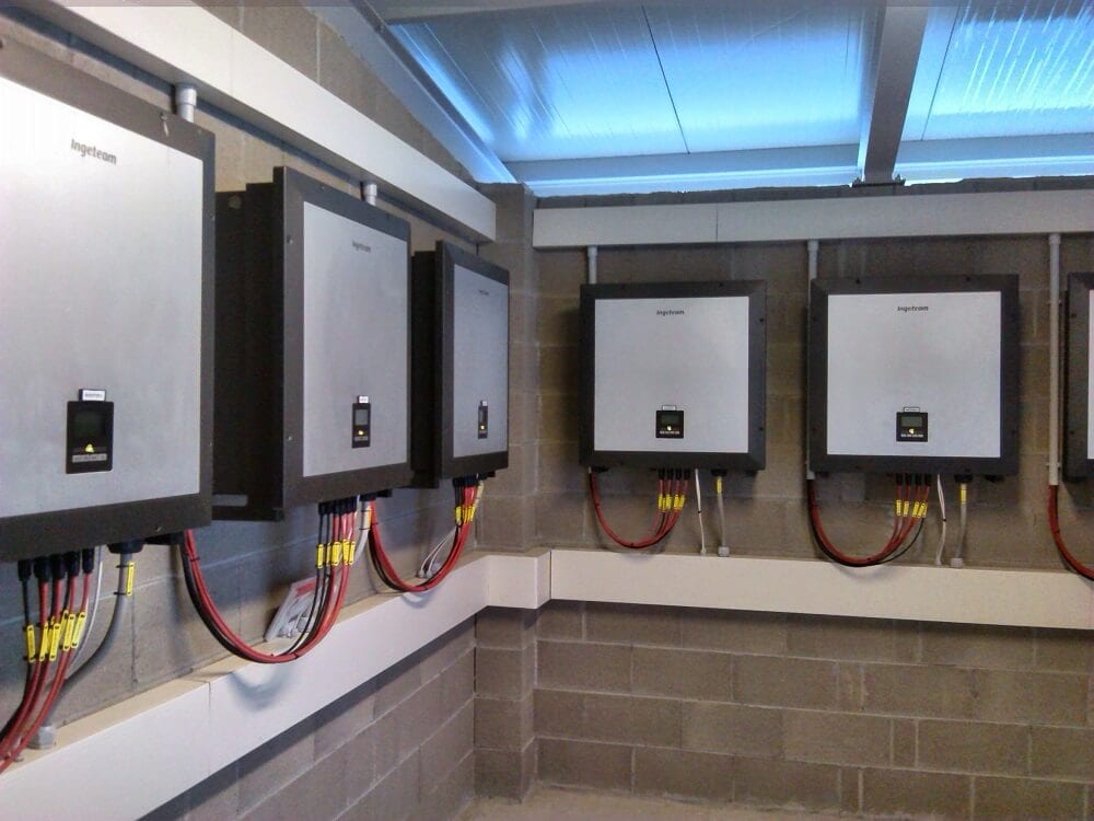
Ingeteam has just launched onto the market its new PV string inverter models, delivering output powers of up to 40 kW in a single inverter. In addition to the 40 kW model, a further three models have also been presented:  24 kW, 28 kW and 33 kW.

The UL version of these models, specifically designed for the North American market, has also been extended to offer output powers of up to 40 kW.

Ingeteam new multiple PV inverter photovoltaic production 40kW 28kW

This is the INGECON SUN 3Play TLMSeries of inverters, noted for their dual MPPT (Maximum Power Point Tracking) as well as their maximum efficiency levels (98.5%) and high performance. For example, this inverter family is suitable for self-consumption systems with no injection of excess energy into the public grid.

Ingeteam has already started to supply these new models to many different markets. The models available until now, with output powers ranging from 10 to 20 kW, are already installed in countries such as Switzerland, Italy, Argentina, Paraguay, France, Australia, Chile, India, El Salvador, Brazil, Mexico, United States and Spain, to mention but a few.

Source

AIXTRON SE, a provider of deposition equipment to the semiconductor industry, has shipped an AIX G5+ C system to French start-up company Exagan, a producer of  gallium nitride (GaN) power switches for electrical converters. The company is a spin-off from Soitec, the SoI (Silicon on insulator) worldwide leader, and CEA-Leti, a European research center focused on micro- and nanotechnologies. Exagan will use Aiwtron’s deposition tool in beginning volume production of gallium nitride on silicon (GaN-on-Si) materials for power-switching devices.

Exagan, in collaboration with its R&D partner CEA-Leti, selected the AIX G5+ C epitaxial deposition tool after evaluating its effectiveness in achieving tight uniformity control and high throughput using Exagan’s proprietary G-Stack™ process technology. This technology is used in creating a unique stack of GaN-based materials that enables the fabrication of Exagan’s G-FET™ transistors. Along with Soitec’s industrial facility and expertise and CEA-Leti’s 200 mm equipment and characterization tools, Aixtron’s equipment adds to Exagan’s supply chain as it ramps up its material production facility in Grenoble.

Fabrice Letertre, COO and Co-Founder of Exagan, comments:

“AIXTRON and our parent company CEA-Leti have enjoyed a long and successful R&D relationship developing GaN-on-Si technology. Now Exagan is partnering with AIXTRON to deliver on our industrial roadmap by using epi to reach our cost milestones. By implementing an efficient GaN-on-Si manufacturing process on 200 mm silicon substrates, we are aligning GaN technology with silicon manufacturing standards. This makes our G-FET products the most cost-efficient wide-bandgap solution for the solar, IT electronics, connectivity and automotive markets.”

Google has finally released the name of Little Box Challenge winner. And the winner is… CE+T Power with it’s Red Electrical Devil’s team (named after the Belgium national soccer team). The judges from Google, IEEE Power Electronics and NREL declared them as far winners of the contest. Second place comes to Schneider Electric and third place to Virginia Tech’s Future Energy Electronics Center.

The Little Box Challenge was a contest launched by Google in July 2014. They promised a 1Million $ prize to whoever was capable of reaching a specific power density. As they described it, the objective was to shrink an Kilowatt-scale inverter in the size of a pizza box, which in other words, comes close to 50W/in³ or 3.05W/cm³.

We already talked about the challenge when it was announced and when the 18 finalists names were released. More than 2,000 teams registered for the competition and the committee reviewed and validated 80 proposals. The 18 finalists had to bring their inverters in person at NREL test lab and go under all listed validations and tests.

According to NREL, most competing teams used either Silicon Carbide (SiC) or Gallium Nitride (GaN) devices. This confirms that reaching this kind of specifications is made way easier using Wide Band Gap devices.

Schneider Electric, Virginia TEch and CE+T Power all built a 2kW inverter that passed all the tests (100 hours on a bench), and matched to the competition specifications. They not only managed to reach the 50W/in³ requirements and challenged it and went way over it.

Google little box challenge results ce+T power schneider electric


Faraday Future, the new Electric Vehicle start-up today announced to have developed and filed patents for high power density inverter. They claim to have increased power density by 20% to 30%.

The FF Echelon inverter patent is the first one to be approved and credited to Faraday Future: U.S. patent #9,241,428 B1

The Inverter was developed by the startup in-house engineering, and led by Senior Director of Electric Drive Silva Hiti.

“Condensing the number of transistors and other complex components enhances the inverter’s overall stability and dependability,” explained Silva Hiti, “allowing us to accomplish far more, with fewer materials.”

The official announcement states that FF team managed to minimize the number of components, both mechanical and electrical pieces, in order to achieve smaller size and higher reliability at the same time. They state that un-even sharing of current across electric components cause higher stress. An issue they solved by having less components to monitor and share current across.

Faraday Future FF Echelon power inverter

This design and method is opposite to the one used by Tesla when they designed and manufactured the first versions model S. As showed and explained in an article we published, Tesla preferred to use proven technology in its inverter, even if the number of IGBTs was high. Tesla used TO-247 discrete packaging for their power semiconductor devices, and managed to monitor and track current in each of these components.

Most Hybrid car manufacturer prefer to use power modules. Toyota designs and manufacture its own power modules and integrates them in the inverter, when most competitors will use Infineon, Mitsubishi Electric, or Danfoss power modules especially designed for electric and hybrid cars.


The new laboratory features a unique, large climate chamber capable of full power electrical testing in conditions simulating the arctic tundra to an equatorial rainforest. In addition, full verification and grid code requirements testing enable ABB to develop larger, more powerful inverters to meet the developing customer and industry trends.

A new multimillion dollar facility designed to test high power central photovoltaic (PV) inverters has been opened in Helsinki. The laboratory supports testing and verification of inverters for safe operation, endurance in a wide range of climatic conditions, compatibility to the most demanding renewables-specific grid code requirements, and to measure and test harmonics and grid interactions.Marc Gomez, Global Product Group Manager for solar inverters at ABB states:

“Our customers are asking for more powerful central inverters. They want to maximize their return on investment and connect more incoming PV power to one inverter. With this lab, we are able to test new inverter concepts, under varying weather conditions, and that allows us to deliver new innovation to our customers and ensure we lead the market.”

Climate testing can last several weeks for the equipment under test. Powered by a DC supply, the inverters are run at varying power levels with different simulated weather conditions to test inverter reliability. The climate chamber allows for accelerated product testing, important when the inverters are typically expected to operate for over 20 years. The climate chamber can vary temperatures from as low as -40°C to as high as +100°C, and relative humidity levels up to 95 percent.

ABB, a leading global supplier of solar photovoltaic inverters, provides the most comprehensive portfolio of products, systems, solutions and services along the solar PV value chain that enable the generation, transmission and distribution of solar power for grid-connected and microgrid applications. The portfolio includes inverters, low-voltage products, monitoring and control systems, grid connection, stabilization and integration products, as well as complete electrical balance of plant solutions. A wide range of support and maintenance services, including remote operations and diagnostics, help ensure solar installations deliver optimal performance.

Source

Fairchild Semiconductor International Inc, said on March 16th it had rejected an acquisition offer from China Resources Microelectronics Ltd and Hua Capital Management Co Ltd, citing concerns over the U.S. approval process.

The move underscores the challenges Chinese companies and investors face in seeking to acquire U.S. chipmakers, particularly when it interferes an existing deals. Fairchild had agreed to sell itself in November to U.S. peer ON Semiconductor for $2.4 billion.

In a filing with the U.S. Securities and Exchange Commission, Fairchild said there was an “unacceptable level of risk” that the deal with the Chinese would be rejected by the U.S. Committee on Foreign Investment in the United States (CFIUS), an inter-agency panel led by the Treasury Department which assesses potential mergers to ensure they do not endanger national security.

China Resources Microelectronics and Hua Capital had offered $2.46 billion for Fairchild in December. Fairchild said that the Chinese offer did not compensate them for the CFIUS risk.

“Specifically, the board believed that the consortium’s proposed $108 million CFIUS reverse termination fee would not adequately justify risking the company stockholder premium present in the ON Semiconductor transaction,” Fairchild said in its filing.

Fairchild’s board is open to another offer by the Chinese, according to a person familiar with the matter who requested anonymity to discuss confidential deliberations.

Fairchild’s decision follows Philips’ scrapping of a plan to sell its Lumileds lighting division to Chinese buyers because of opposition from CFIUS in January.

Some lawyers who specialize in CFIUS transactions have advised clients that Chinese investments in U.S. high tech companies will have difficulty winning approval from the notoriously opaque CFIUS, unless the Chinese buyer is truly private, said Jim Lewis of the Center for Strategic and International Studies who follows CFIUS.

“Any company reading the tea leaves will see that it’s going to be a bumpy ride getting CFIUS approval for a Chinese investment in the semiconductor industry,” he said. In particular, the Defense Department and Department of Homeland Security worry about supply chain security, he said.

U.S. touchscreen chip maker Synaptics Inc, is currently in talks with a Chinese group of investors about being acquired.

Source

Veeco Instruments Inc., the world’s leading supplier of metal organic chemical vapor deposition (MOCVD) systems, announced today that it has signed a joint development project (JDP) agreement with imec, the Belgium-based nano-electronics research center.  The collaboration is expected to accelerate the development of highly-efficient, Gallium Nitride (GaN) based, power electronic devices using GaN Epi wafers created using Veeco’s Propel® Power GaN MOCVD system.

Imec has already demonstrated significant gains in GaN layer uniformity and run-to-run repeatability with Veeco’s Propel system, resulting in significantly improved power device yields.  The single wafer reactor incorporates Veeco’s proprietary TurboDisc® technology that delivers superior film uniformity, run-to-run control and defect levels compared to batch reactors.

“Within the framework of our industrial affiliation program on GaN-on-Si, Veeco and imec have collaborated over the last four years to improve the Epi quality of GaN layers deposited on silicon wafer substrates,”

said Rudi Cartuyvels, Senior Vice President Smart Systems and Energy Technologies at imec.  “The ultimate goal is to produce the next generation of highly efficient power switching devices. We have set very high GaN device yield and reliability targets for 2016 and we look forward to partnering with Veeco to achieve these targets.”

Learn more about Power electronics Gallium Nitride devices and applications markets reading our report here.

“We are very pleased with our imec collaboration,” said Jim Jenson, Senior Vice President and General Manager, Veeco MOCVD Operations.  “Global demand for advanced power electronics with greater energy efficiency, a smaller form factor and greater reliability is rapidly accelerating.  We believe that the technology in our Propel single wafer system will enable imec to achieve their power device targets and help to bring these advanced devices to market faster.”

Basic 3C Inc., a Longmont startup aiming to go to market soon with a new type of semiconductor, has added about $650,000 from existing investors to a Series A round of funding.

Basic 3C president Bart Van Zeghbroeck said this week that the hope is that the latest funds get the company through the next six months before raising a Series B.

Founded in April 2014, the company — based at 1830 Boston Ave. — has been in product-development mode, but is hoping to commercialize its first product in the next six months.

Basic 3C’s semiconductors will be made from cubic silicon carbide, rather than silicon. Geared toward high-power applications operating at 600 volts or more that require efficient power conversion, the product will have higher thermal conductivity and do well in “operationally rugged environments,” Van Zeghbroeck said. He said targeted applications include solar panels, wind turbines and electric vehicles. A reduced cooling requirement would mean reduced size and weight and thus, in something like an electric vehicle, improved efficiency and range.

“We’re looking at significantly better material properties, and that makes a difference in the end application,” Van Zeghbroeck said.

Investors in the company include Boulder-based Infield Capital and Texas-based Dankat LLC.

Van Zeghbroeck is on leave from the University of Colorado, where he has been an electrical engineering professor since 1990. He and investors purchased the technology and intellectual property for Basic 3C from a Golden company, Silicon Carbide Systems, that had gone bankrupt.

Van Zeghbroeck said Basic 3C will initially do manufacturing at its current space in Longmont. The company has fewer than 10 employees, but he said he expects that number to grow to 15 or 20 within the next 18 months.

Sanken Electric has expanded its lineup of SiC Schottky diodes. The new FMDA-10565 SiC Schottky is rated for 650V and 5A with a typical forward voltage drop of 1.5V at 25°C. Taking advantage of the high speed switching capability of SiC, these diodes achieve reduced switching loss, and reduced reverse leakage current at high temperatures. At 25°C, typical leakage current is 15 µA at a junction temperature of 150°C, typical leakage current is 70 µA.

he FMDA-10565 is designed for use in PFC sections, motor drive circuits and inverters in applications such as servers, communications power equipment, air conditioners, and so on. Packaged in a TO220F-2L, these Schottky’s have a temperature coefficient of 2.5°C/W and an operating junction temperature range of -40 to 175°C.

These devices are particularly well-suited for continuous current mode PFC circuits. They are capable of reducing the power loss that results from the recovery current. The diode’s high-speed switching capability and energy-saving functionality allows for the potential downsizing of equipment. The 5A FMDA-10565 is the third device in this family and it joins the 10A FMCA-11065 and the 20A FMCA-22065.