IXYS Corporation announced an expansion of its Ultra Junction Power MOSFET product line: 650V X2-Class Power MOSFETs with fast body diodes. With on-resistance as low as 17 mΩ and current ratings ranging from 22A to 150A, these devices are optimized for soft-switching resonant-mode power conversion applications.

The intrinsic fast body diodes of the MOSFETs display very soft recovery characteristics, minimizing electromagnetic interference (EMI) especially in half or full-bridge switching topologies. With low reverse recovery charge and time, the body diodes can be utilized to make sure that all the energy are removed during high-speed switching to avoid device failure and achieve high efficiency.

Like other Ultra Junction MOSFETs from IXYS, these new devices have been developed using a proprietary process technology resulting in Power MOSFETs with significantly reduced on-resistance and gate charge. They also exhibit a superior dv/dt performance and are avalanche rated as well. Thanks to the positive temperature coefficient of their on-state resistance, they can be operated in parallel to meet higher current requirements.

Suitable applications include resonant-mode power supplies, high intensity discharge (HID) lamp ballast, ac and dc motor drives, dc-dc converters, robotic and servo control, battery chargers, 3-level solar inverters, LED lighting, and Unmanned Aerial Vehicles (UAVs).

These new 650V X2 Power MOSFETs with HiPerFET™ body diodes are available in the following international standard size packages: TO-220, TO-263, SOT-227, TO-247, PLUS247, TO-264, and PLUS264.

Some example part numbers include IXFA22N65X2, IXFH46N65X2, IXFK120N65X2, and IXFN150N65X2, with drain current ratings of 22A, 34A, 120A, and 145A, respectively.

Automotive electronics specialist HELLA, in collaboration with GaN Systems, and charging technology researchers at Kettering University’s Advanced Power Electronics Lab have developed a Level-2 electric vehicle (EV) charger prototype with efficiencies exceeding 97% at an unprecedented 2.6 kW/l power density. Prior to this achievement, Level-2 EV chargers reached maximum efficiencies of 94%. Using GaN Systems’ 60 A, 650 V GS66516T switches in an innovative two-stage architecture, the Kettering University research team, led by Associate Professor of Electrical Engineering, Dr. Kevin Bai, were able to increase the wall-to-battery efficiency to more than 3% greater than previously obtained.

HELLA’s Manager of Advanced Engineering, Matt McAmmond, added,

“The results of this collaboration are equally gratifying and commercially important, because they provide HELLA with a path to ultra-compact and lighter EV charger designs. In addition to benefiting HELLA and our customers, this development also has a positive environmental impact, as it represents another step toward the global effort to reduce power consumption.”

Dr. Bai and his team are known for collaborating with companies to help advance their charging technology. Commenting on the importance of this development, Dr. Bai said, “The switching performance we observed with the GaN Systems’ parts was marvelous. Using these devices our power electronics exhibited a power density greater than 2.6 kW/l. This is a significant milestone with important implications for charging electric vehicles, among other charging applications.” Dr. Bai characterized this development as a ‘game changer’ for the EV charging industry.


Gruppo PBM, a leader in industrial battery chargers, is using SiC MOSFETs in its new HF9 battery charger family to enable higher efficiency and power density at a lower overall system cost.

Demand for safe, efficient and fast-charging industrial batteries has increased exponentially along with the proliferation of power electronics. The HF9 product family is designed to provide the highest possible efficiency while achieving easy scalability for power ranging from six to 16 kilowatts. These benefits are made possible in part by Wolfspeed 1200V SiC MOSFET technology.

“We selected Wolfspeed SiC Planar MOSFETs for our new HF9 battery charger family because they enabled us to improve our battery chargers while achieving operational savings, increased productivity and increased safety. This was not possible with the best IGBTs in the market,”

said both Marco Mazzanti and Giancarlo Ceo, who respectively serve as CTO and R&D Engineer at Gruppo PBM.

Based in Italy, Gruppo PBM specializes in rugged high-frequency battery chargers, dischargers and testers. By using Wolfspeed SiC MOSFETs in its latest HF9 family, Gruppo PBM not only achieves improved efficiency, but also a reduction in component count, improving the overall reliability in the system by lowering the operating temperatures and—most importantly—reducing overall system cost.

“Wolfspeed’s SiC MOSFETs, especially our new C3M 900V family, are enjoying rapid adoption in the growing battery charger market segment,” explained Edgar Ayerbe, Wolfspeed’s power MOSFET marketing manager. “Our products increase power density and dramatically lower switching losses, making it possible to introduce smaller, cooler and lower cost chargers for the automotive and industrial markets.”

Sourcehttp://www.wolfspeed.com/news/gruppo-pbm

Game changing new technology delivers bi-directional AC/DC power flows, combining the functions of a rectifier, an inverter and a transfer technology in a single module.

Eltek is today announcing the launch of the Rectiverter, a power conversion module combining the functions of a rectifier, an inverter and a “static transfer switch” in one. The Rectiverter is a 3-port bidirectional converter that simplifies solutions providing both AC and DC power to critical loads in telecom, data center and industrial applications. It features a power conversion efficiency of 96% in mains mode and 94% when operating as an inverter.
Combining a rectifier, which converts AC to DC, and an inverter, which converts DC to AC into one box simplifies the power system complexity, reduces system size and improves overall system reliability, resulting in a reduced total cost of ownership over the product lifetime.

Eltek’s first product on the market is the Rectiverter HE, delivering 230V/1500W AC and 48V/1200W DC. It features high power conversion efficiency, and is controlled by a single Eltek Smartpack controller. Rectiverter systems are available as single or 3 phase, input and output, and can be scaled to meet any power demand.

“The Rectiverter is the first new technology development in modular power conversion for many years and it’s a big step into more efficient, more reliable power infrastructure,”

said Morten Schoyen, chief marketing officer of Eltek.

“It is a product that fits in well in applications where we today use rectifiers and inverters separately, and will open doors to new exciting opportunities”

“To integrate a rectifier and an Inverter in the same box, with bidirectional power flow and still maintain high efficiency is an impressive achievement,” said Dr. Tore M. Undeland, Prof Emeritus of Electrical Engineering at Norwegian University of Science and Technology (NTNU).
The Rectiverter first version is based on 48VDC and has a maximum capacity of 1500 VA for AC and 1200W of DC.  The total capacity of a module is 2000VA (AC and DC combined).

Source

POWDEC has succeeded in making GaN PSJ (Polarized Super Junction) transistors on sapphire substrate having both 1,200 V rating-voltage and the on-resistance of less than 100 mΩ.

Powdec has developed a PSJ (Polarization Super-junction) structure instead of the FP (Field-Plate). The PSJ is so strong against the current collapse that sapphire can be used as substrate. As a result, the device is free from the electric breakdown caused by the substrate. And Powdec succeeded in obtaining up to 6 kV of the breakdown voltage for the device with GaN thickness as thin as 1 μm.

GaN-on-Si devices are applied to the conversion systems only below 600 V rating range. However, the present achievements using the unique PSJ-on-sapphire platform shows that the PSJ devices can enter into the application fields where Si-IGBTs dominate today.

What is Polarized Super Junction?

SJ (Super-junction) is a structure to improve both the conductivity and the breakdown voltage of the Si power-MOS transistor. The drift layer consists of thin p/n stacks while the conventional one consists of a single n-type layer. PSJ (Polarization Super-junction) is a method to implement the SJ effect in the GaN/AlGaN system where the polarization effect functions as SJ.

GaN-on-Silicon versus GaN-on-Sapphire:

Most GaN device makers develop GaN-on-Silicon (or GaN/Si) power devices. Powdec’s 1,200V devices are GaN-on-Sapphire devices. Not using the Silicon and using Sapphire implies intrinsic differences in the device structure and operation.

GaN-on-Si power devices:

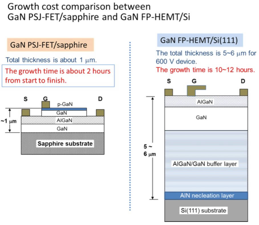
GaN power devices today are implemented on Si(111) substrate, which is called “GaN-on-Si” or “GaN/Si”. The thickness of the nitride layers needed for 600V rating devices is generally 5μm or more. The GaN/Si devices are equipped with Field-plates (FP are conductive plates set on the gate to split the steep electric field). FPs are indivisibly needed for the conductive Si substrate to mitigate the current collapses. Current-collapse is another name for the current decreasing phenomenon during the transistor operation. The channel electrons are scattered and deployed around the channel by the strong electric field. These immobile electrons act as the negative bias for the channel resulting in the decrease of the current.

Advantages of GaN-on-Sapphire for Power devices:

Powdec GaN on sapphire gallium nitride power devices PSJ super junctionSapphire substrate is also a common platform for GaN-LED production and the growth runs successively without chamber-cleaning. On the other hand, the growth on Si substrate needs chamber-cleaning prior to the deposition to avoid the unwanted chemical reactions between GaN and Si interface. The chamber-cleaning takes extra time and cost. As a whole, the throughput for GaN PSJ-FET/sapphire growth is roughly ten times larger than that of the GaN FP-HEMT/Si growth.

The thermal conductivity of sapphire, 40 [W/m K], is lower than that of Si, 150 [W/m K]. This problem is solved here by face-downing the die and contacting it on the base substrate, so that the heat can dissipate without going through the sapphire. As a result, the device has operated at as large as 8 amperes of the continuous current mode (CCM) under free standing (without fin) condition.


The company HeSaLight has just booked no less than 50,000 power converters at Nordic Power Converters:

Nordic Power Converters is a spin-out company based on several years of technology development at DTU Electrical Engineering. The newly developed power converters that are both smaller and much more durable than traditional power converters are to be used in LED luminaires which HeSaLight manufactures.

The large order and a capital investment of DKK 13m from Seed Capital and 10 other investors means that Nordic Power Converters can now expand the business and hire more employees. Thus the company can really get started with producing tomorrow’s power converters, which could also replace the current big and bulky power converters for PCs for instance. Earlier this year Nordic Power Converters won Danish Tech Challenge – a competition for hardware-based companies and EU’s prize EIT Venture Award.

source

EpiGaN, the leading European supplier of  6- and 8-inch GaN-on-Silicon epi-wafers for 600-V HEMT (High Electron Mobility Transistor) power semiconductors, and SunEdison Semiconductor, a manufacturer of silicon substrates for semiconductor manufacturing, have signed a global representation agreement for EpiGaN’s GaN-on-Si epi wafers.

The terms of the global representation and distribution agreement between EpiGaN and SunEdison Semiconductor grant SunEdison Semiconductor exclusive rights for the marketing and sales of EpiGaN’s 150mm and 200mm GaN-on-Si Epiwafers for power switching applications, substantially strengthening EpiGaN’s worldwide reach and transition EpiGaN into a global GaN epiwafer supplier.

EpiGaN, located in Hasselt, Belgium, is a global player in developing III/V materials and delivers GaN-on-Si epi-wafers to semiconductor device manufacturers worldwide. EpiGaN’s product portfolio covers power switching applications up to 650V as well as RF power devices for millimeter-wave applications. EpiGaN is today developing and sampling GaN structures on 200mm Si substrates for power switching devices to enable its customers to successfully position themselves in rapidly growing market segments.

A key concept of EpiGaN’s advanced technology base is the in-situ SiN cap layer, which provides best-in-class passivation properties and superior device reliability. The use of in-situ SiN allows the use of pure AlN layers as barrier material with the resulting heterostructures having sheet resistance values below 300 Ohm/sq. Combining EpiGaN’s differentiating GaN-on-Si technology with SunEdison Semiconductor’s market presence and expertise will create a new one-stop solution for IDMs active in next-generation GaN power technology on Si substrates.

“This new agreement with a well established supplier such as SunEdison Semiconductor, with its excellent track record in the power electronics industry, will enable us to provide additional value to our global customer base through our superior GaN-on-Si products, customer services & technical support,”

said Dr Marianne Germain, cofounder and CEO of EpiGaN.

“We are proud to collaborate with the EpiGaN team,” commented Shaker Sadasivam, SunEdison Semiconductor’s President and CEO. “EpiGaN’s strong technology capability compliments our own, and we look forward to further developing this promising market together.”

Source

FINsix Corporation , the high-frequency power electronics design start-up, today announced its partnership with Lenovo, the PC manufacturer, to bring Lenovo’s laptops the smallest ever 65W charger option for ThinkPad laptops.

The two companies have collaborated under a joint development agreement, and Lenovo is set to offer the new charger, dubbed the ThinkPad 65W Adapter, as an option for the new ThinkPad X1 Carbon and X1 Yoga. FINsix and Lenovo will be exhibiting the new charger at CES, the global consumer electronics trade show, January 6-9 in Las Vegas.

FINsix is a company Point The Gap featured in its article about Gallium Nitride and consumer power adapters. It developped a laptop adapter using Resonant LLC converter topology to operate at higher frequency of conversion. This high frequency allows smaller passive components and better efficiency. It’s a technology transferred from RF and Military applications. FINsix was initially created on the campus of MIT, with the objective to power LED with their technology. They reoriented their aim to laptop adapters later, as a more accessible market. These technology will be featured in Point The Gap next market report about GaN devices and applications.

An interesting fact about this technology is that today’s FINsix adapters use Infineon Silicon based devices (CoolMOS and OptiMOS, respectively for high voltage and low voltage sides). But it could become and enabler and a first volume produced system to use Gallium Nitride power electronics devices. The topology fits perfectly the high frequency capabilities of GaN devices. It also compensates the youngness of GaN with the relatively short lifetime needed for a laptop charger.

“Lenovo is constantly searching for partners who have disruptive technologies that can add value to our customers,” said Luis Hernandez, vice president and general manager of Lenovo’s ThinkPad Business Unit. “We are working with FINsix because their power conversion technology is a game-changer. It brings a level of portability that we expect will become the standard of the future.”

Vanessa Green, CEO of FINsix, said,

“We are thrilled to partner with the market leader in personal computers. Lenovo has a strong customer base and this collaboration positions us to scale quickly among corporate customers eager to lighten their load when on the go.”

The ThinkPad 65W Micro Adapter is based on the same high-frequency power technology as FINsix’s first product, the Dart, a 65W aftermarket laptop adapter with a 2.1 amp USB port for simultaneously charging phones, tablets, and other devices. The Dart has been featured in a Kickstarter campaign about 18 months ago. Deliveries have been delayed many times and does not seem to have started yet. It was featured at CES in 2014.


The new facility produces and develops Insulated Gate Bipolar Transistor (IGBT) modules, which are terminal power semiconductor devices used as electronic switches that combine high efficiency and fast switching, IMI said in a statement.

They are used on trains, refrigerators, lamp ballasts, air-conditioners, solar applications, motion devices and anything that needs electric switching and requires power efficiency.


“The power module business is very much aligned with IMI’s strategy of offering innovative solutions which will impact our top and bottom lines. Further, it is in line with the expanding business in our target markets of automotive and industrial segments,” IMI President and Chief Executive Officer Arthur Tan was quoted in the statement as saying.

IMI is one of the few companies in the world capable of handling not only the electronics manufacturing side of the power modules but also the power semiconductor side of the business, Mr. Tan said.

Power modules are seen accounting for 30% of the total power of semiconductor market by 2019, IMI said.

Demand for modular power solutions from original equipment manufacturers is on the rise because of their higher power density and reliability, IMI said.

The company refurbished a surface mount technology assembly facility in Laguna Technopark into a power module facility, IMI Strategic Planning and Marketing Manager Frederick L. Blancas said.

IMI reported a 5% year-on-year jump in nine-month profit to $22 million despite a global economic slowdown and electronics industry downturn that pulled down consolidated revenues by 4% to $621.5 million.

Shares in IMI added four centavos or 0.69% to close at P5.80 each on Thursday.

Source

As part of the company’s strategy to move more significantly into power semiconductors for industrial and automotive markets, Littelfuse has made an investment in Monolith Semiconductor, Inc., a start-up company developing silicon carbide technology. Silicon carbide is a rapidly emerging semiconductor material that enables power devices to operate at higher switching frequencies and temperatures versus conventional silicon. This allows inverters and other energy conversion systems to be built with significantly improved power density, energy efficiency and cost.

“Investing in and partnering with Monolith’s experienced team of silicon carbide and power semiconductor experts allows us to quickly evolve our portfolio with strategically relevant and innovative technology,”

said Ian Highley, Littelfuse Senior VP and GM, Semiconductor Products, and CTO.

“Silicon carbide power technology is among the most promising advancements in the semiconductor market today. It will be an important tool in helping us solve complex problems for our customers.”

“Forming this strategic partnership with Littelfuse accelerates development and helps bring silicon carbide technology to the market,” said Sujit Banerjee, PhD, CEO of Monolith Semiconductor. “Littelfuse is an ideal partner for us. We are excited to dramatically increase our customer reach, gain access to global channels, and benefit from their sales and marketing depth and expertise.”

Initially this is not a material investment for Littelfuse; however, the company has committed to add to its investment once Monolith has achieved certain milestones. This investment is not expected to have any material financial impact on Littelfuse in 2015 or 2016.

About Littelfuse
Founded in 1927, Littelfuse is the world leader in protection with growing global platforms in power controls and sensing. The company serves global customers in the electronics, automotive and industrial markets with technologies including fuses, semiconductors, polymers, ceramics, relays and sensors. Littelfuse has over 8,000 employees in more than 35 locations throughout the Americas, Europe and Asia. For more information, please visit the Littelfuse website: Littelfuse.com.

About Monolith Semiconductor
Monolith Semiconductor Inc., a Round Rock, Texas-based startup company, is focused on improving the affordability and reliability of SiC power devices by utilizing advanced manufacturing techniques and high-performance processes and designs. For more information, please visit the Monolith Semiconductor website: monolithsemi.com.

Source

Raytheon UK’s foundry has received an order from a major fabless semiconductor manufacturer to mass produce silicon carbide (SiC) Schottky barrier diodes which are used for power conversion.

Raytheon UK’s Scottish facility will produce over 1,000 wafers in the first year. The customer will package the devices, which will have voltage ratings ranging from 600V to 1.7kV and current ratings ranging from 1 to 50A.

“This order demonstrates the increasing demand for silicon carbide semiconductors,” said John Kennedy, head of Raytheon UK’s Integrated Power Solutions.

“We have the process know-how and we’re adept at minimising the engineering costs. As an independent foundry, we have greater scope to find more innovative solutions for our customers.”

Raytheon UK’s Glenrothes foundry is the longest established independent full-scale production-qualified facility in Europe – if not the world – capable of SiC wafer processing. It has, for example, already fabricated Schottky and PiN diodes, as well as JFETs and MOSFETs, for other customers.

SiC properties include a breakdown electric field of 2,000kV/cm compared to silicon’s 300kV/cm – allowing for higher voltages; a bandgap energy of 3.26eV compared with silicon’s 1.12eV – enabling RUK007 Page 2 of 2 DECA-613 higher temperature operation; and excellent thermal conductivity (4.9W/cm.K compared with silicon’s
1.5W/cm.K).

source

World-leading nano-electronics research center imec announced today that it is extending its Gallium Nitride-on-Silicon (GaN-on-Si) R&D program, and is now offering joint research on GaN-on-Si 200mm epitaxy and enhancement mode device technology. The extended R&D initiative includes exploration of novel substrates to improve the quality of the epitaxial layers, new isolation modules to increase the level of integration, and the development of advanced vertical devices. Imec welcomes new partners interested in next generation GaN technologies and companies looking for low-volume manufacturing of GaN-on-Si devices to enable the next generation of more efficient and compact power converters.

“Since the program’s launch in July 2009, we have benefited from strong industry engagement, including participation from IDMs, epi-vendors and equipment and material suppliers. This underscores the industrial relevance of our offering,” stated Rudi Cartuyvels, executive vice president of smart systems at imec. “Interested companies are invited to become a partner and actively participate in our program. Imec’s open innovation model allows companies to have early access to next-generation devices and power electronics processes, equipment and technologies and speed up innovation at shared cost.”

GaN technology offers faster switching power devices with higher breakdown voltage and lower on-resistance than silicon, making it an outstanding material for advanced power electronic components. Imec’s R&D program on GaN-on-Si was launched to develop a GaN-on-Si process and bring GaN technology towards industrialization. Building on imec’s excellent track record in GaN epi-layer growth, new device concepts and CMOS device integration, imec has now developed a complete 200mm CMOS-compatible GaN process line. Imec’s GaN-on-Si technology is reaching maturity, and companies can gain access to the platform by joining imec’s GaN-on-Si industrial affiliation program (IIAP). The process line is also open to fabless companies interested in low-volume production of GaN-on-Si devices tailored to their specific needs, through dedicated development projects.

Imec’s portfolio includes three types of buffers optimized for breakdown voltage and low traps-related phenomena (i.e. current dispersion): a step graded AlGaN buffer, a super lattice buffer, and a buffer with low-temperature AlN interlayers. Imec explored side-by-side enhancement mode power devices of the MISHEMT and p-GaN HEMT type, as well as a gate-edge terminated Schottky power diode featuring low reverse leakage and low turn-on voltage.

The latest generation of imec enhancement mode power devices shows a threshold voltage beyond +2V, an on-resistance below 10 ohm mm and output current beyond 450 mA/mm. These devices represents the state of the art of enhancement mode power devices.

In this next phase of the GaN program, imec is focusing on further improving the performance and reliability of its current power devices, while in parallel pushing the boundaries of the technology through innovation in substrate technology, higher levels of integration and exploration of novel device architectures.

source