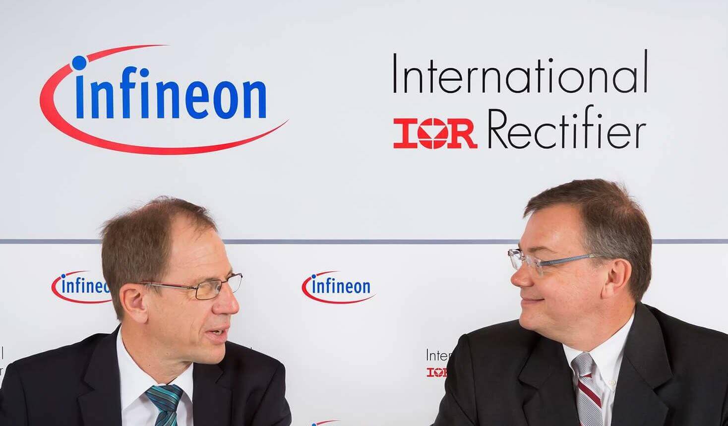
Infineon Technologies AG announced today the closing of the acquisition of International Rectifier. With effect from today, the El Segundo based company has become part of Infineon following the approval of all necessary regulatory authorities and International Rectifier’s shareholders.

“The acquisition of International Rectifier is an important step for Infineon to foster our position as a global market leader in power semiconductors. We are sure that International Rectifier and its employees will make a great contribution to a joint successful future. Together both companies make a powerful combination”

, says Dr. Reinhard Ploss, CEO of Infineon. “We offer our customers an unparalleled product portfolio. Our profound understanding of their needs enables us to provide the best possible and competitive solutions. The acquisition helps us to accelerate our strategic approach ‘from product thinking to system understanding’.”

The combined company is led by Reinhard Ploss, CEO, Arunjai Mittal, Member of the Management Board Regions, Sales, Marketing, Strategy Development and M&A, and Dominik Asam, CFO. President of International Rectifier and of Infineon North America is Robert LeFort.

International Rectifier is highly complementary to Infineon: the combined company gains greater scope in product portfolio and regions, especially with small and medium enterprise customers in the US and Asia. The merger taps additional system know-how in power management. It expands the expertise in power semiconductors, also combining leading knowledge in compound semiconductors, namely Gallium Nitride. Furthermore, the acquisition will drive greater economies of scale in production, strengthening the competitiveness of the combined company.

Merger background

On August 20, 2014, Infineon had announced that it was to acquire International Rectifier in a deal worth approximately USD 3 billion. The Board of Directors of International Rectifier and Infineon’s Supervisory Board unanimously supported the offer of Infineon to pay USD 40 per outstanding share. Subsequently, all regulatory authorities had approved the acquisition – as did the shareholders of International Rectifier with a majority of 99.5 percent of all votes cast.

Ploss_Khaykin-IFX-IR-cut

Source

The SuperGrid Institute is one of several energy-transition projects promoted and part funded by the French government. It is a collaborative research institute bringing together public and private organisations to develop new technologies for supergrids.

The SuperGrid Institute’s work will make an important contribution to the transition to low-carbon energy. To dramatically increase the share of renewable energy in the energy mix, future transmission grids will have to offer a special combination of capabilities not available today: long-distance transmission (to connect remote renewable energy sources), subsea or underground energy transport, the ability to handle unpredictable fluctuations in renewable energy generation, and more. Meshed HVDC grids are a promising solution to these issues, but they require that a number of technological challenges be overcome. And that is the ambition of the SuperGrid Institute.

Supergrid institute smartgrid grid HVDC Alstom

“Today, the institute is hosted primarily at the Alstom complex at Villeurbanne, France. However, we are in the process of building
our own campus with buildings, equipment and test facilities. In fact, we envisage making our test facilities commercially available to
third parties. The same is true of the intellectual property (IP) we generate.”

“We already have some patents in the pipeline and we shall leverage our IP assets to forge new partnerships and generate licence income.”

Says Philippe Auriol, retired professor of the Ecole Centrale Lyon and former director of a CNRS laboratory

“A key point for universities and students is the proximity of test and measurement facilities on high-power, high-voltage prototypes. Very few university labs have access to this type of equipment – anywhere in the world. These tests and measurements will then constitute the starting point for new basic research projects.
Some PhD research projects are currently under way. For example, a ‘fail-to-short’ project – a packaging technique to ensure that a failed electronic module is seen as a short circuit. Another is focusing on the control of high-voltage power electronics to ensure a high level of insulation.”

Says Hervé Morel, Senior Scientist at Université de Lyon

Jean-François Ballet, Managing Director of the SuperGrid Institute and Vice-President Industry Projects at Alstom Grid, explains:

“We have structured the SuperGrid Institute into five key programmes to achieve our ambitious goals.”

  • Programme 1: Supergrid system architecture, operation and control
  • Programme 2: Technologies for breaking, insulation and measurement
  • Programme 3: Power conversion technologies
  • Programme 4: Supergrid cables and lines
  • Programme 5: Stabilisation and storage


Source

“Taking into account the increasing challenges IGBT technology is facing, we are very pleased to present a package that answers the needs of our industry both for today and for the foreseeable future.”

Infineon Technologies AG today announced the launch of two new power module platforms designed to improve the performance of high-voltage IGBTs in voltage classes from 1200V up to 6.5kV. To make the benefits of the new module broadly available, Infineon is offering a royalty-free license of the design to all providers of IGBT power modules. First products using the platform concept will include the high voltage classes 3.3kV (450A%

SBE is designing a fully size-and-performance compatible DC Link system for the HP Drive IGBT module in collaboration with Infineon. Both vertical and horizontal connection systems will be available. The vertical system is designed to occupy the same footprint as the HP Drive itself and the horizontal system will respect the shorter length of the new HP Drive. This way, customers will be able to take full advantage of the size reduction offered by the improved Infineon technology and trust in the demonstrated performance and lifetime capability of the SBE Power Ring Film Capacitor technology.


The SSBE Capacitor on IGBT PackBE DC Link system is fully capable of supporting the voltage and current options that can be used with the new Infineon HP Drive module. Yet the size is greatly reduced from conventional DC Link systems used today with the larger HP2 module systems. The SBE system insures that the customer can actually realize the potential inverter power density improvement which can be facilitated by the Infineon HP Drive.
SBE is known in the industry as providing the highest ripple current density available. There is no need to sacrifice the capability of this exciting product development by Infineon by using standard technology offerings for the required DC Link system.

SBE will have sample systems available at the time of release of the Infineon HP Drive and prototype and preproduction systems over the coming months. Starting in 1Q15, you will be able to order these products on the SBE on line store. However, as we expect demand for these initial prototypes to be high, you are welcome to pre-order by contacting customer service at jaimeb@sbelectronics.com.

Source: http://www.sbelectronics.com/2014/12/collaboration-infineon-optimized-dc-link-designfor-new-hp-drive-6-pack-igbt-module/

Mitsubishi Electric corporation announced today it will begin work on the development of standardized-package high-power semiconductor modules for use in heavy industry, including traction and electric-power applications, aiming to offer an optimal design for energy savings and high efficiency in high-power electronics systems.

Design Concept of High-Power Module with New Package

  • Common package design for modules of up to 6.5kV rating
  • Simple, easy parallel connection realizes various current ratings
  • Package compatibility with products of Infineon Technologies AG (Germany)


The first products to incorporate the new design platform will be for the high-voltage classes 3.3kV (450A), 4.5kV (400A) and 6.5kV (275 A). The standardized package will measure 100mm x 140mm x 40mm.

High-power modules are key devices used in power systems of between several kW and several MW. High-current modules with maximum ratings of 6.5 kV exist already. The industrial power market requires diverse modules suited to various current and voltage ratings according to each system’s power-conversion capacity. Products with compatible package dimensions from multiple manufacturing sources are also in demand.

Mitsubishi Electric intends to satisfy these market demands with its new high-power modules. Further details will be introduced in power electronics-related exhibitions, such as TECHNO-FRONTIER in Japan and Power Conversion Intelligent Motion Europe in Germany, both of which will be held in May 2015.

The global AC drives manufacturer Vacon is now part of the Danfoss Group, effective 1 December 2014. In September 2014, Danfoss announced a public tender offer to acquire all the shares of Vacon. By the end of November, Danfoss obtained approvals from all the relevant authorities, and has now acquired more than 90% of Vacon shares and voting rights in Vacon.

Danfos and Vacon logos

The combination of Vacon and Danfoss will create one of the world’s leading players in the drives market, leveraging the best of the two companies.

“The clear ambition is to be a leading player in the drives market. We see that true value is created together. This is why we will create a new business, where people work together to develop the best products, applications and services for our customers,” says Niels B. Christiansen, President and CEO of Danfoss.

“Combining two strong and innovative AC drives companies will give customers an even more competitive, innovative and attractive offering of AC drives. Joining forces also means that the new business will be able to invest further in both R&D and in the sales force, which is a key success factor in our business,” says Vesa Laisi, President and CEO of Vacon.

Vesa Laisi will be the President of the new business segment, named Danfoss Drives.

“The dedicated drives focus unites both Vacon and Danfoss and distinguishes the two companies from competitors.”

“Vesa has spent most of his career in the drives industry and he possesses very deep insights into the business. He will use this experience to guarantee world-leading product portfolio and customer service,” says Niels B. Christiansen.

Danfoss also announces a reorganization of the rest of the Group. The closing of the Vacon deal now paves the way for establishing four strong and global segments.

“Today, we have very strong businesses and with the new structure, we can unite these in even stronger entities to further strengthen our market positions.”

“This is the right outset for the next part of our strategic journey with a strong focus on growth,” says Niels B. Christiansen.


Source

TF Semiconductor Solutions Inc of Roseville, CA, USA has completed its spin-off as an independent company after being the Products Division of TSI Semiconductors Inc (formerly Telefunken Semiconductors America), a specialty analog and mixed‐signal foundry.

With design centers in Torrance, CA and Dover, NH, USA, TF Semi is capitalizing on many years of investment in product, IP research & development work from its original high-voltage integrated circuit (HVIC) efforts at Telefunken.

TF Semi is focusing on designing and manufacturing devices for the high-voltage power management market – where its HVIC devices have already won designs with motor and power supply manufacturers – as well as LED drivers, LVDS interface devices, and JTAG system testing solutions. In particular, as well as high-side & low-side drivers, half-bridge drivers and 3-phase drivers, the portfolio includes what is claimed to be the industry’s first 200V enhancement-mode gallium nitride (eGaN) driver, the TFG1200. TF Semi also offers a Specialty Products portfolio with devices targeting the LVDS interface, JTAG system test and power management for high-reliability applications.

Source: http://www.semiconductor-today.com/news_items/2014/SEP/TFSEMI_050914.shtml

Solectria Renewables, LLC, a leading U.S. PV inverter manufacturer, and Yaskawa Electric Corporation announced today that the companies have reached a definitive agreement whereby Yaskawa Electric will acquire Solectria Renewables through its U.S. subsidiary, Yaskawa America Inc.  Solectria Renewables will continue to operate as a wholly owned subsidiary.

Headquartered in Lawrence, Massachusetts, Solectria Renewables manufactures high performance photovoltaic (PV) inverters for residential, commercial and utility-scale power systems.  Since being founded in 2005, Solectria has grown to become a leader in the North American solar market. The Company employees over 170 people throughout the U.S.

Founded ninety-nine years ago, Yaskawa Electric is a $3.6 billion global leader in factory automation solutions, and has also established a leadership position in the low power PV inverter market in Japan.

This acquisition will benefit Yaskawa and Solectria customers alike.  Yaskawa will bring scale, global sales and manufacturing facilities as well as diversification to Solectria.  Likewise Solectria will bring over 25 years of power electronics experience, ten dedicated to the PV industry, and an in depth knowledge of medium and high voltage PV products to Yaskawa.

Yaskawa America’s President and COO Mike Knapek explains:

“This is an effort to broaden Yaskawa’s exposure in the renewable energy market and expand the use of our technology expertise.  Solectria has built a strong and successful organization in the Solar Inverter market over the past 10 years.  The philosophies and strategies of both organizations are highly aligned on enabling sales growth and market expansion through superior customer experiences.  We are very excited to bring Solectria into the Yaskawa family to provide world leading Inverter solutions.”

Solectria Renewables’ CEO, James Worden said:

“While this is a significant step for Solectria, I am even more thrilled about what this means for our customers. They will have the same management team and personal interaction they are accustomed to, with the advantage of a powerful diversified global partner.  Our entire team should feel incredibly proud about we have built over the past 10 years, but the best is yet to come.”

About Solectria Renewables, LLC:

Solectria Renewables, LLC of Lawrence, Massachusetts, is a leader in the development and manufacturing of a wide range of inverters for renewable power applications including 1.8 kW to 750 kW grid-tied PV inverters for systems from 1 kW to multi-megawatts. Solectria Renewables’ products are backed by more than 25 years of experience in the power electronic and inverter industries and are supported by world class warranties. All of Solectria Renewables’ three-phase inverters, string combiners, and web-based monitoring components qualify as Made in the USA. To learn more about Solectria Renewables, please visit http://www.solectria.com.

About Yaskawa America Drives and Motion Division:

Yaskawa America is a wholly owned subsidiary of Yaskawa Electric Corporation, founded in 1967, the Drives & Motion Division provides industrial control and automation products to markets in the Americas.  North American based operations include R&D, design and product engineering and two assembly plants producing inverters, servo motors and custom industrial panels.  Yaskawa is the world’s largest manufacturer of AC drives and motion control products, including adjustable frequency drives, servo amplifiers, servomotors, machine controllers and motion controllers.  Drives and servo systems are applicable to a wide variety of automation tasks in a wide variety of industries.  With every new generation of design, products are given more features, more flexibility and more adaptability to more applications.

About Yaskawa Electric Corporation:

Yaskawa Electric Corporation located in Kitakyushu, Japan is a world leader in factory automation solutions.  Founded in 1915, Yaskawa Electric has provided exceptional customer experiences for almost 100 years. Focusing on mechatronic solutions, it has shipped over 20 million AC inverters, 13 million Servo’s and 290,000 robots worldwide.

Full SiC Dual in-line power factor available today:

Mitsubishi Electric Corporation announced today the immediate launch of a transfer-molded super-mini dual in-line package power factor correction (DIPPFCTM) module incorporating silicon carbide (SiC) transistors and diodes, which is expected to help reduce the power consumption and size of home appliances.

Mitsubishi Electric’s new DIPPFC module will be exhibited at MOTORTECH JAPAN 2014 during TECHNO-FRONTIER 2014, which will be held at Tokyo Big Sight in Japan from July 23 to 25.

Product Features

  1. SiC contributes to lower power consumption and compact size
      • Power loss is reduced by about 45% compared to silicon (Si) products, contributing to improved energy conversion.
      • SiC schottky-barrier diode (SBD) reduces recovery current power consumption and electromagnetic interference noise.
      • SiC metal oxide semiconductor field effect transistor (MOSFET) achieves maximum 40kHz high-frequency switching and contributes to downsizing of peripheral components, such as reactors and heat sinks.
      • Power factor correction (PFC) and driving IC contribute to downsizing by reducing mounting surface area and simplifying wiring.
  2. Simplified design for inverter systems
      • Interleave method for PFC decreases the ripple current and simplifies the noise filter circuit.
      • Adoption of the same package as the dual in-line package intelligent power module (DIPIPMTM) simplifies the installation of heat sinks.

Hidden inside nearly every modern electronic is a technology — called power electronics — that is quietly making our world run. Yet, as things like our phones, appliances and cars advance, current power electronics will no longer be able to meet our needs, making it essential that we invest in the future of this technology.

Today, President Obama will announce that North Carolina State University will lead the Energy Department’s new manufacturing innovation institute for the next generation of power electronics. The institute will work to drive down the costs of and build America’s manufacturing leadership in wide bandgap (WBG) semiconductor-based power electronics — leading to more affordable products for businesses and consumers, billions of dollars in energy savings and high-quality U.S. manufacturing jobs.

Integral to consumer electronics and many clean energy technologies, power electronics can be found in everything from electric vehicles and industrial motors, to laptop power adaptors and inverters that connect solar panels and wind turbines to the electric grid. For nearly 50 years, silicon chips have been the basis of power electronics. However, as clean energy technologies and the electronics industry has advanced, silicon chips are reaching their limits in power conversion — resulting in wasted heat and higher energy consumption.

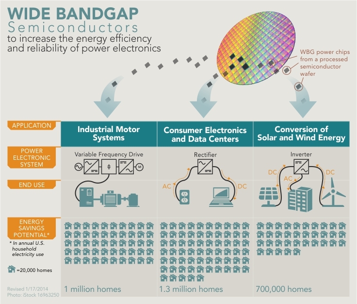
Wide band gap infrographics

Power electronics that use WBG semiconductors have the potential to change all this. WBG semiconductors operate at high temperatures, frequencies and voltages — all helping to eliminate up to 90 percent of the power losses in electricity conversion compared to current technology. This in turn means that power electronics can be smaller because they need fewer semiconductor chips, and the technologies that rely on power electronics — like electric vehicle chargers, consumer appliances and LEDs — will perform better, be more efficient and cost less.

One of three new institutes in the President’s National Network of Manufacturing Innovation, the Energy Department’s institute will develop the infrastructure needed to make WBG semiconductor-based power electronics cost competitive with silicon chips in the next five years. Working with more than 25 partners across industry, academia, and state and federal organizations, the institute will provide shared research and development, manufacturing equipment, and product testing to create new semiconductor technology that is up to 10 times more powerful that current chips on the market. Through higher education programs and internships, the institute will ensure that the U.S. has the workforce necessary to be the leader in the next generation of power electronics manufacturing.

Watch our latest video on how wide bandgap semiconductors could impact clean energy technology and our daily lives.

Source: http://energy.gov/eere/articles/infographic-wide-bandgap-semiconductors

Dynex headquarter

Dynex headquarter

Dynex Semiconductor today announced that its parent company, Zhuzhou CSR Times Electric Co Ltd. held a ceremony at its facility in China to mark the opening of a new $240 million IGBT production base in Zhuzhou. The new production base, the first of its kind in China, and the second worldwide, will produce high-power IGBT chips and modules using 8-inch silicon. Annual output of the first phase of this new production line is expected to reach 120,000 wafers and 1 million pieces of IGBT modules. This IGBT line is being operated by the newly formed Semiconductor Business Unit of CSR Times Electric, of which Dynex is the European subsidiary.

 The technology being used in the new facility has been developed at Lincoln in the UK by the multinational CSR Zhuzhou R&D Center based at Dynex Semiconductor Ltd. The UK R&D centre was established in 2010 to focus on leading edge power semiconductor technology and specifically the next generation of IGBT products. CSR began construction of the new 8-inch production line in May 2012. Throughout the build, equipment installation and commissioning Dynex has played a leading role in providing technical advice, support and staff training both in Lincoln and in China.

 The IGBT is the key component in today’s energy efficient electric energy conversion systems used in electric locomotives, metros, electric and hybrid electric vehicles, electric power grids and renewable energy plants. Using the latest silicon wafer fabrication equipment and the latest process technologies, the new line will initially produce high power modules using the latest soft punch through field stop and trench technologies.

 Dr Paul Taylor, President and CEO of Dynex Commented:

“Since the acquisition of Dynex by CSR Times Electric in 2008 there has been a rapid development in our IGBT capability. We began with 4-inch wafers, then up graded to 6-inch at our plant in Lincoln. We then extended our technology to support the design of this new facility. It complements our base in the UK by giving us access to a world leading 8-inch IGBT wafer fabrication facility and a high volume module assembly line”

 “Our rapid development does not stop there “continued Dr Taylor “the new line has been kitted out with the latest equipment, and the next phase of expansion is already being planned. This targets key markets such as electric automotive and renewable energy. So at our UK R&D Center we are already working on designing the next generation of advanced silicon and silicon carbide power devices, and are busy recruiting new staff to expand our multinational research, design and development teams to meet this exciting new challenge”

Source: http://www.powerpulse.net/story.php?storyID=30347

Applied Materials CEO Gary Dickerson, left, and Tokyo Electron Chairman and CEO Tetsuro (Terry) Higashi, right, unveil ‘Eteris™,’ the new name of their combined company once the merger is approved, at an event on Monday, July 7, 2014, in San Francisco, Calif.​

Applied Materials, Inc. and Tokyo Electron Limited today unveiled the new name and logo of their combined company which will be used once the merger closes. Derived from the concept of eternal innovation for society, Eteris(TM) [pronounced: eh-TAIR-iss] embodies the spirit of what will drive the new company and speaks to what makes the combination unique.

“The new name for our combined company builds on the strong legacies of Applied Materials and Tokyo Electron, creating something even greater than the sum of the two,” said Tetsuro Higashi, chairman, president and CEO of Tokyo Electron. “At the time we announced our plans to merge, we said this was a bold step forward for our industry. The name Eteris demonstrates our commitment to a new and exciting future for our company to create and enable technology innovations that improve the way people live.”

Eteris is innovative and forward-looking and our logo symbolizes expanding future opportunities driving a new era of innovation and growth,” said Gary Dickerson, president and CEO of Applied Materials. “With a new name, mission and vision, we are bringing our new company into focus so that we can move quickly, execute our combined strategy and begin to create value as soon as the merger closes.”

Eteris captures the company’s focus on innovations that will enable its customers and move the industry forward. Core to Eteris is the promise to leave a positive and lasting impact on the world. Paired with the name is a bold logo that celebrates Eteris‘ role in realizing the incredible possibility of technology. At the heart of the mark, the bright green square symbolizes the energy of the new company, the power of its technology and the foundation of innovation it provides to enable customer success. From the green foundation, bright colors and new dimensions expand, representing the many innovations Eteris will make possible every day. The logo represents expanding future opportunities that drive new innovation and growth.

 The unveiling of the new company’s name and logo are the latest milestones in the merger’s progress. Last month the stockholders of Applied Materials and Tokyo Electron declared strong support for the combination. Approximately 99% of the shares voting at the Applied Materials stockholder meeting and 95% of the shares voting at the Tokyo Electron stockholder meeting voted to adopt the proposed business combination. These results underscore the value the combination brings to stockholders.

 The closing of the business combination remains subject to customary conditions set forth in the parties’ Business Combination Agreement, including review by regulators in various countries. Applied Materials and Tokyo Electron expect the transaction to close in the second half of 2014.

 Forward-Looking Statements

This communication contains forward-looking statements, including but not limited to those regarding the proposed business combination between Applied Materials and Tokyo Electron (the “Business Combination”) and the future performance of their combined businesses. Forward-looking statements may contain words such as “expect,” “believe,” “may,” “can,” “should,” “will,” “forecast,” “anticipate” or similar expressions, and include the assumptions that underlie such statements. These statements are subject to known and unknown risks and uncertainties that could cause actual results to differ materially from those expressed or implied by such statements, including but not limited to: the ability of the parties to consummate the Business Combination in a timely manner or at all; satisfaction of the conditions precedent to consummation of the Business Combination, including the ability to secure regulatory approvals in a timely manner or at all; Applied Materials’ and Tokyo Electron’s ability to successfully integrate their operations, product lines, corporate structures, transfer pricing policies, technology and employees and realize expected synergies, savings and growth; the level of demand for the combined companies’ products, which is subject to many factors, including uncertain global economic and industry conditions, demand for electronic products and semiconductors, and customers’ new technology and capacity requirements; Applied Materials‘ and Tokyo Electron’s ability to (i) develop, deliver and support a broad range of products, expand their markets and develop new markets, (ii) timely align their cost structures with business conditions, and (iii) attract, motivate and retain key employees; and other risks described in  Applied Materials’ filings with the Securities & Exchange Commission, Tokyo Electron’s filings with the Financial Services Agency of Japan, and the registration statement on Form S-4 filed with the SEC by TEL-Applied Holdings B.V. and declared effective on May 13, 2014. All forward-looking statements are based on management’s estimates, projections and assumptions as of the date hereof. Except as required under applicable law, none of Applied Materials, Tokyo Electron or TEL-Applied Holdings undertakes any obligation to update any forward-looking statements.

 About Applied Materials

Applied Materials, Inc. (Nasdaq: AMAT) is the global leader in precision materials engineering solutions for the semiconductor, flat panel display and solar photovoltaic industries. Our technologies help make innovations like smartphones, flat screen TVs and solar panels more affordable and accessible to consumers and businesses around the world. Learn more at www.appliedmaterials.com.

 About Tokyo Electron

Tokyo Electron Limited (TSE: 8035), established in 1963, is a global supplier of semiconductor and flat panel display production equipment, and a provider of technical support and services for semiconductor, flat panel display and photovoltaic panel production equipment worldwide. TEL has located research & development, manufacturing, sales, and service locations all over the world. http://www.tel.com