X-FAB is set to become a leader in the SiC devices production. Following their announcement in October last year, they did what they said. The Lubbock, Texas manufacturing site is now offering SiC devices production on 6 inches wafers, in addition to its 30K Si Wafer production capacity.

X-FAB not only invested capital to upgrade the fab. They also got the help of PowerAmerica Institute and NC State University. As a result, the following production tools have been added : high-temperature anneal furnace, backgrind equipment for thinning SiC wafers, backside metal sputter and backside laser anneal tools. A high-temperature implanter will be installed later this year.

The production capacity is of 5k wafers/month and can potentially be extended further.

Source

Transphorm, one of the best-known Gallium Nitride power electronics start-ups has officially opened its”Center of Excellence” in San Jose, California. A team was established and growing for one year in Silicon Valley. It’s now official. The Center will also have worldwide offices.

The objective was to support and educate customers about the GaN transistor technology and how to design using this new wide band gap material based devices. Center’s staff will also build a knowledge base made of white papers, reference designs and publications.

Transphorm, like many of its competitors, now needs to educate and evangelize the market. It’s required to accelerate adoption of GaN Devices, and avoid the long and slow adoption of SiC MOSFET we have seen for the past 5 years.

The fuse and protection systems maker Littelfuse has increased its investment in Silicon Carbide. They already took part in the SiC business by investing in Monolith Semiconductor in December 2015. They increased their participation in the start-up of $15M to become the major investor.

This move fully integrates with the company’s strategy to enter the semiconductor market. They secured more standard technology production by acquiring a part of  ON Semiconductor. More precisely, the new “TVS” and “IGBT” product lines of Littelfuse were the former diodes, thyristors and Automotive IGBT activities of ON Semiconductor. Littelfuse also planned to invest $30M in production facilities improvement.

With this new investment, Littelfuse can now be considered as part of the main power semiconductor manufacturers. The Silicon Carbide market, which took time to establish. It has been difficult to manufacture components in mass and to drag costs down. It is now beginning to be real. Littelfuse grabbed the opportunity to be part of the next generation power semiconductor market.

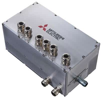
Mitsubishi announced that their team developed an ultra-compact Full Silicon Carbide (SiC) inverter, targeting HEV (Hybrid & Electric Vehicle) applications. They claim it to be the world smallest with a volume of 5 litres.

The power density is 86 kVA/L, which is 10x more than CE+T Power, winner of the Google Little Box Challenge, with exactly 8.85 kW/L.

Mitsbishi Electric SiC inverter electric hybrid vehicle

Mitsubishi did not release more technical details than the picture up here. On the other side, they claimed to use solder to connect power semiconductors and cooling elements, in order to reach the best performance and lifetime. Commercialization is not planned before 2021… But more technical details will come during the National Convention of the Institute of Electrical Engineers (IEEJ) from March 15-17, 2017.


Navitas, innovating start-up in WBG semiconductor, has announced the release of the first fully integrated IC in Gallium Nitride. It’s based on their AllGaN transistor platform.

Navitas is targetting charging solutions, fast-chargers and small power high-end converters with this half-bridge building block. GaN based transistor are able to operate at much higher frequency, with lower losses than currently used solutions for these converters: Super Junction MOSFET.

GaN transistor Navitas half-bridge IC

The NV6250 is a 650V half-bridge with intergrated Navitas driver technology iDrive. It switches at up to 2Mhz, all packed in 6x8mm QFN package.

Production is planned for Q2 2017 (which is very soon…).

After acquiring International Rectifier in January 2015, Infineon signed an agreement to acquire Wolfspeed in July 2016 for $850 M. This agreement has first been put on hold by the CFIUS (Committee on Foreign Investment in the United States). The Committee required guarantees on several national security concerns about leaving Wolfspeed in the hands of a non-US company.

As a reminder, the SiC (Silicon Carbide) device maker Wolfspeed was spin-off from Cree in May 2015, and renamed in September of the same year. The objective for Cree was to run their RF and Power electronics activities separately from the LED activities. The two businesses have different gowth rates and investment needs.

The new entity came after Cree acquired APEI (Arkansas Power Electronics Inc.), a North Carolina-based company designing high-performance and high-efficiency converters. APEI’s activity was probably the source of these concerns, as most of their commercial activity is directly linked with military applications of power electronics converters, DoD (Department of Defence) being in need of such systems.

Source

[EDIT: Infineon’s attempt to buy Wolfspeed is terminated since February 16th 2017.]

Wolfspeed, former power electronics division of Cree, has expanded its line of SiC (Silicon Carbide) MOSFETs. Generation 3, also called C3M(r) platform, features lower inductance and RdsON.

The 1200V device comes in addition to the 900V and 1000V devices previously available. It also comes in a new package as surface-mount 7L D2PAK, available in a few weeks. The more classics 4L TO-247 and SMD packages are already available, with respectively C3M0075120K and C3M0075120J part numbers. It’s a 30 A maximum current MOSFET, with as low as 75 mΩ RdsON.

For more details, you can check the datasheet here.


Navitas Semiconductor announced the immediate availability of production qualified iDrive™ Gallium Nitride (GaN) Power ICs using the company’s proprietary AllGaN™ technology. The NV6131, NV6105 & NV6115 offer a high-efficiency 650V, 160mOhm power FET with increasing integration of digital and analog circuits, leading to ground breaking speed, energy efficiency, power density and reduced system cost.

GaN can enable up to 100x higher frequencies than silicon but driving, controlling & protecting such high-speed power devices has been an industry challenge that has limited adoption.  By integrating these critical digital and analog circuits monolithically with the GaN power device, these system level problems have been eliminated. Navitas GaN Power ICs with iDrive guarantee optimized & robust performance for any application. A 10-100x increase in system operating frequency is combined with higher efficiencies to enable up to a 5x increase in power densities and 20% lower system costs.

“GaN Power ICs, with the monolithic integration of logic, analog & power, represent an industry breakthrough that will change the landscape of power electronics as we know it”, explained Navitas CEO Gene Sheridan.  “By integrating all gate-drive-related circuitry, virtually all frequency-related power losses are eliminated, opening the door to significant frequency and efficiency gains.  We anticipate a major upgrade cycle in mobile fast chargers, thin TVs, high-efficiency data centers, LED lighting, solar and electric vehicle markets as this new high-speed revolution in power electronics gets underway”, Sheridan added.

“The Center for Power Electronics Systems (CPES) at Virginia Tech has been pioneering the advancement of high-frequency power systems for over three decades” explains Dr. Fred Lee, the university’s distinguished and globally recognized professor. “The invention of GaN power ICs represents a major industry breakthrough and is a critical ingredient to make high-speed, high-efficiency power systems a reality.  This is an exciting time for the power industry”, Lee concluded.

STMicroelectronics has extended its SLLIMM™ nano series of Intelligent Power Modules (IPMs) for motor drives with more package options that help minimize overall size and complexity, extra integrated features, and greater efficiency leveraging the latest-generation 500V MOSFETs.

With a current rating of 1A or 2A, the new IPMs target applications up to 100 Watts, such as refrigerator compressors, washing-machine or dishwasher motors, draining and recirculation pumps, fans, and other drives running at less than 20kHz in hard-switching circuitries. Operation up to 150°C allows use in harsh environments.

The modules integrate a three-phase MOSFET bridge and gate-driver HVICs, with value-added features including an unassigned op-amp and comparator for functions such as over-current protection and current sensing. Additional built-in safety features include interlocking to prevent shoot-through currents from damaging MOSFETs of the bridge, a fault-status output, shutdown input, and smart-shutdown capability. An optional built-in thermistor helps simplify over-temperature protection.

In addition to the zig-zag lead option, the new series is also available in a line-lead package. These give designers extra flexibility to simplify the board layout and minimize controller size in mechatronic assemblies and other space-constrained applications.

The high thermal performance of the packages, combined with the superior efficiency of ST’s latest 500V MOSFETs, enhances designers’ freedom to minimize heatsink size or create heatsink-free solutions for lower-power applications. The low MOSFET on-resistance of 3.6Ω and 1.7Ω, in 1A and 2A variants, respectively, combines with low switching losses to ensure high overall energy efficiency. The MOSFETs have separate open-emitter connections to module pins, which simplifies use of three-shunt current sensing for field-oriented motor control (FOC) or single-shunt sensing for trapezoidal control. The modules also integrate the bootstrap diodes needed to control the high-side MOSFET gates, further minimizing demand for external components.

The STIPN1M50T-H, STIPN1M50-H, STIPN2M50T-H (L), and STIPN2M50-H are in production now, priced from $4.50 in the Dual Inline Package for orders of 1000 pieces.

For further information please visit www.st.com/ipm

Source

Toshiba Corporation’s Storage & Electronic Devices Solutions Company today announced the launch of second generation 650V silicon carbide (SiC) schottky barrier diodes (SBDs) that improve on the surge forward current (IFSM) offered by the company’s current products by approximately 70%. Shipments of the new line-up of eight SiC schottky barrier diodes start today.

The new SiC schottky barrier diodes, fabricated with Toshiba’s second-generation SiC process, deliver approximately 70% better surge forward current than first generation products, and at the same time reduce the switching loss index of “RON*Qc” by around 30%, making them suitable for use in efficient power factor correction (PFC) schemes.

The new products are available in four current ratings of 4A, 6A, 8A, and 10A, either in a non-isolated “TO-220-2L” package or an isolated “TO-220F-2L” package. These products can contribute to improving the efficiency of power supplies in devices including 4K large screen LCD TVs, projectors and multifunction copiers, and in industrial devices such as telecommunication base stations and PC servers.

Package Characteristics
(Ta=25℃)
Absolute Maximum Ratings Electrical Characteristics
Forward DC Current Non-repetitive Peak Forward Surge Current Total Power Dissipation Forward Voltage Anode-cathode
On-resistance
Junction Capacitance Total Capacitive Charge
Symbol IF(DC) IFSM Ptot VF Ron Cj QC
Value Max Max Max Typ.
&Max
Typ. Typ. Typ.
Unit (A) (A) (W) (V) (mΩ) (pF) (nC)
Test Conditions/
Part Number
@ Half-sine Wave
t=10 ms
@IF(DC) @IF(DC)×
0.25 to 1.0
@VR=1 V @VR=400 V
Non- Isolation
TO-220-2L
TRS4E65F 4 39 55.6 1.45
(Typ.)
1.60
(Max)
120 165 10.4
TRS6E65F 6 55 68.2 82 230 15.1
TRS8E65F 8 69 83.3 62 300 19.7
TRS10E65F 10 83 107 48 400 24.4
Isolation
TO-220F-2L
TRS4A65F 4 37 33.6 1.45
(Typ.)
1.60
(Max)
120 165 10.4
TRS6A65F 6 52 35.4 82 230 15.1
TRS8A65F 8 65 37.5 62 300 19.7
TRS10A65F 10 79 39.7 48 400 24.4

Source

VisIC Technologies, an innovator of efficient power electronics based on Gallium Nitride (GaN) semiconductors, announced today that it has closed $11.6 million in a Series C financing lead by a new investor Birch Investment with participation of existing investors.
The revolutionary potential of GaN-based electronics for electrical power delivery systems, from consumer power supplies to solar inverters, UPS, power supplies for Cloud/Data Centers and electric motor drives, has been marketed and anticipated for years, especially for high voltage and high current switching applications. VisIC Technologies is the company that demonstrated performance of high current GaN switching device and 1200V GaN power switch.

“We are very excited by the level of support provided by VisIC’s new and existing investors, who share our vision for the extraordinary potential of VisIC’s GaN based products. It is an important milestone for our company. Having achieved the best performance metrics for any GaN devices in the market, this new capital infusion positions us to accelerate commercialization and dominate the market segment.”

said Tamara Baksht, VisIC Technologies’ founder and CEO.

About VisIC Technologies:
Based in Nes Ziona, Israel, VisIC Technologies, Ltd. was established in 2010 by experts in Gallium Nitride (GaN) technology to develop and sell advanced GaN-based power conversion products. VisIC has successfully developed, and is bringing to market, high power GaN-based transistors and modules. (GaN is expected to replace most of the Silicon-based (Si) products currently used in power conversion systems.) VisIC has been granted keystone patents for GaN technology and has additional patents pending.
For more information:  www.visic-tech.com

Panasonic, which recently launched mass production of its X-GaN process of lateral GaN HeMT, presented a 1.7kV GaN device during IEDM conference. GaN devices available today are limited to 650V for enhancement mode devices, and 1200V for depletion-mode normally-on devices. Panasonic’s device demonstrated during IEDM is a GaN/GaN Vertical device having a Ron of 1mΩcm².

The device is based on a V-shaped structure, and a secondly grown GaN/AlGaN interface separated from the first one, which improves electron mobility by a factor of 5. Panasonic’s team also used a carbon doped GaN layer to avoid punch-through phenomenon.

Source