Infineon celebrated the Grand Opening of its new warehouse and Gallium Nitride (GaN) cleanroom at its Mesa facilityin Arizona, (USA). The multi-million-dollar expansion project added approximately 11,500 sq. ft. to the existing facility.

Dr. Juergen Woehl, Managing Director, Infineon Epi Services, said, “As a leader in semiconductor technology, our Mesa facility underlines Infineon’s commitment to work on advanced materials here in Mesa and we were delighted to celebrate the expansion of our site with our executives, employees and state and local representatives.”

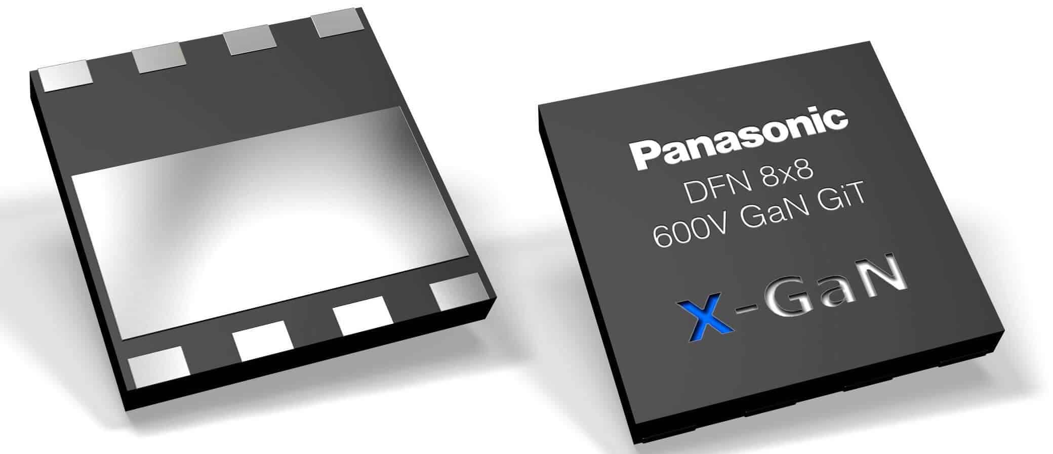
Infineon Gallium Nitride GaN facility Mesa ArizonaInfineon acquired a ready for production GaN technology together with it’s acquisition of International Rectifier. But this technology is more adapted to the lower voltage range, up to 400V. They also signed and agreement to manufacture a Gallium Nitride high voltage power devices technology from a license and act a second source for X-GaN, Panasonic’s GaN technology. As stated in our GaN market report, The bigger companies are not the only players weighting in the newly coming Wide Band Gap semiconductor business. They have to fight against start-ups as GaNSystems, Transphorm, EPC corp, ViSiC and many other. We expect this facility expansion to be made to fuel the manufacturing of X-GaN technology.


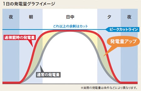
Omron Corp announced that it will release the “KPM2” PV inverter suited for “overloading,”  in December 2016.

‘Overloading’ is a feature that allows this single-phase PV inverter to  handle more panels that it’s rates power announces in order to maximize elecricity production during mornings, evening or small sunlight moments.

Omron overlaod production curve example

Ormon presentation of the Overload feature

Maximum input voltage is 450V DC, and maximum current is 11A. It is a single-phase PV inverter for outdoor use. It is designed for residential and small-scale solar power installations.

As a result, it becomes possible to ensure business feasibility even with a low purchasing price (FIT tariff), the company said. Omron plans to sell 300,000 units during the next 3 years.


Transphorm Inc., a GaN (gallium nitride) semiconductors designer and manufacturer, today announced its latest portfolio addition: the TPH3212PS. Available in a TO-220 package, the device has an on-resistance of 72 mOhms (mΩ).

To date, Transphorm’s product portfolio consists of 600V and 650V discrete FETs spanning TO-220, TO-247, and PQFN88 packages for power levels up to 4.5 kilowatts. The TPH3212PS fills a power level gap in the company’s second generation product line, specifically between the 52mΩ and 110mΩ FETs.

“Transphorm aims to enable the market by delivering GaN in the highest quality, highest reliability format as possible,” said Umesh Mishra, CTO, Transphorm.

“We recognize GaN is not just a drop-in replacement for silicon MOSFETs used today. Board redesign and system modifications are required to capitalize on GaN’s complete set of benefits from performance through to system cost. If we can minimize that learning curve by working with well-known packages and a configuration that behaves similarly to a MOSFET—we believe the industry will move further faster.”


Availability, Pricing and Support

Fully-qualified and in production, the TPH3212PS is priced at US$8.94 in 1000-unit quantities. The product is currently supported by a SPICE program and application notes. A full evaluation kit for 2.5 kilowatt hard-switched half-bridge, buck or boost designs is available for pre-order and priced at US$250. Visit here for details.

Panasonic Corporation today announced that it will start mass production of a high-speed gate driver (AN34092B) optimized for driving its GaN power transistor X-GaN in November 2016. The company will also start mass production of two types of X-GaN (PGA26E07BA and PGA26E19BA) and provide solutions in combination with high-speed gate drivers.

GaN gallium nitride power device transistor market production

GaN is one of the next generation semiconductor compounds that can achieve space and energy savings when applied to transistors used in various power units. A gate driver is required to drive a transistor; however, general gate drivers for conventional silicon (Si) transistors cannot exploit the potential of GaN transistors since the gate structure of GaN transistors is different from that of Si transistors.

The new high-speed gate driver (AN34092B) helps our X-GaN easily and safely achieves high-speed switching performance. It can drive transistors at high frequencies of up to 4 MHz and integrates the active miller clamp function that prevents malfunction during high-speed switching. X-GaN achieves a 600 V breakdown enhancement mode through our unique technology and features high-speed switching and low on-resistance. The combination of X-GaN and dedicated high-speed gate drivers will contribute to significant space and energy savings of various power conversion units for industrial and consumer use.

X-GaN and dedicated high-speed gate drivers are suitable for various applications such as 100 W to 5 kW power supply units, inverters, data centers, mobile base stations, consumer electronics, audio-visual equipment, industrial and medical devices.

Source

Qualcomm Inc. and NXP Semiconductors today announced a definitive agreement, unanimously approved by the boards of directors of both companies, under which Qualcomm will acquire NXP.  Pursuant to the agreement, a subsidiary of Qualcomm will commence a tender offer to acquire all of the issued and outstanding common shares of NXP for $110.00 per share in cash, representing a total enterprise value of approximately $47 billion.

NXP is a leader in high-performance, mixed-signal semiconductor electronics, with innovative products and solutions and leadership positions in automotive, broad-based microcontrollers, secure identification, network processing and RF power.  As a leading semiconductor solutions supplier to the automotive industry, NXP also has leading positions in automotive infotainment, networking and safety systems, with solutions designed into 14 of the top 15 infotainment customers in 2016.  NXP has a broad customer base, serving more than 25,000 customers through its direct sales channel and global network of distribution channel partners.

“With innovation and invention at our core, Qualcomm has played a critical role in driving the evolution of the mobile industry.  The NXP acquisition accelerates our strategy to extend our leading mobile technology into robust new opportunities, where we will be well positioned to lead by delivering integrated semiconductor solutions at scale,”

said Steve Mollenkopf, CEO of Qualcomm Incorporated.  “By joining Qualcomm’s leading SoC capabilities and technology roadmap with NXP’s leading industry sales channels and positions in automotive, security and IoT, we will be even better positioned to empower customers and consumers to realize all the benefits of the intelligently connected world.”

The combined company is expected to have annual revenues of more than $30 billion, serviceable addressable markets of $138 billion in 2020 and leadership positions across mobile, automotive, IoT, security, RF and networking.

Investor presentation deck is available here


Source

Acquisition will enhance Murata’s position as a world’s leading provider of high reliability capacitors

Murata Manufacturing Co., Ltd.,  and IPDiA S.A. today announced that Murata Electronics Europe B.V., a wholly-owned subsidiary of Murata is about to acquire  IPDiA, a 3D silicon capacitor technology pioneer headquartered in France, and IPDiA will become a subsidiary of Murata. The transaction is expected to close before the end of October.
This acquisition will enhance Murata’s position as the leading provider of high reliability capacitors. It is part of Murata’s strategy to strengthen its core business within the communication (mobile) market, and to expand into new applications within the automotive and medical markets.
IPDiA, headquartered in Caen, France, was formed in 2009 and has around 130 employees today. The company is dedicated to the manufacturing of leading edge Integrated Passive Devices, specializing in silicon sub-mounts for lighting and 3D silicon capacitors for medical, industrial, communication and high reliability applications. The company operates design centers, sales and marketing offices and a manufacturing facility (silicon wafer FAB) for the automotive market and for medical devices.
As a result of this acquisition, IPDiA will be integrated into Murata, and IPDiA’s products and solutions will be commercialized as part of Murata’s product portfolio.

“Combining IPDiA’s 3D silicon capacitor technologies with Murata’s current technologies and product portfolio will enable us to expand our combined offering and meet our customers’ high reliability requirements, such as high temperature or high voltage, in automotive and other demanding markets”

, says Toru Inoue, Executive Vice President, Components Business Unit, Murata. In addition, Franck Murray, IPDiA CEO   commented,

“In the last 7 years, we have worked intensively to establish and strengthen our presence in the electronics industry. IPDiA’s patented technology has enabled silicon passive components to be considered as a superior solution in specific markets where high performance and miniaturization are required. We wish to benefit from Murata’s  world recognized expertise and sales force  to further expand  our products and business. We look forward to working with Murata to enhance their leading position in the passive market”.

IPDiA in brief

IPDiA is a leading manufacturer of Integrated Passive Devices. Its technology has been adopted by world leaders in medical electronics, semiconductor area and high reliability industry.
IPDiA portfolio includes silicon capacitors from pF to tens of µF with:

  • High Reliability Medical and Automotive Grade Capacitors;
  • Low Profile Capacitors < 80 µm thin for decoupling inside critical space application;
  • High Temperature Capacitors (250°C) with very high stability;
  • Ultra Broadband Capacitors (60+GHz);
  • 2D/2.5D Silicon Interposers for integration in SiP or MCM;
  • Passive component networks for integration in module or on board.

CISSOID, the leader in high-temperature and extended lifetime semiconductor solutions, announces cooperation with Data Device Corporation (DDC), the world leader in the design and manufacture of high-reliability data bus, motion control, and solid state power controller products for aerospace, defense, and industrial applications, and with its subsidiary Beta Transformer Technology Corporation (BTTC), the leader in high performance military, commercial and space-level magnetic components, for the development of more compact and reliable Silicon Carbide (SiC) MOSFET Intelligent Power Modules (IPM) for Aerospace power converters and motor control.

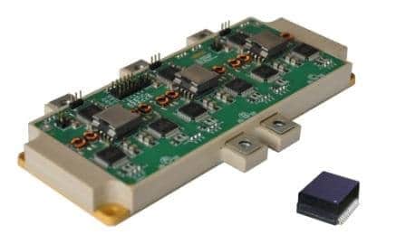
Within this partnership, BTTC will develop high reliability and high temperature transformer modules, embedding both power and pulse transformers, optimized for CISSOID HADES2®  Isolated Gate Driver. This solution will be used in SiC MOSFET Intelligent Power Modules (IPM) developed by CISSOID, making them more compact and reliable. It will address SiC IPM developed for high power density applications (see picture) but also IPM in hermetically sealed packages currently in development for harsh environments, e.g. unpressurized locations and/or extreme temperatures.

SiC high temperature Cissoid Avionics power module

First transformers modules are being developed, validated and qualified for temperature ranges from -55°C and up to +225°C. Magnetic cores and other transformer materials have been carefully selected to offer a stable behaviour and a reliable operation within this range. The transformers will provide isolation in excess of 2500Vdc and are optimized for very low parasitic capacitances in order to support high dV/dt, typically up to 50KV/µs, common with fast switching SiC transistors. These transformers have been optimized to work with HADES2®  Isolated Gate Driver chipset: the power transformer is used inside a Flyback DC-DC converter supplying both low- and high-side isolated gate drivers while pulse transformers are transmitting PWM and Faults signals.

“With DDC and BTTC, we found the right partners to develop high reliability and high temperature transformer solutions for our SiC IPM and gate drivers. They bring to CISSOID their long experience in developing signal and power transformers for data transceivers and power converters as well as their high quality manufacturing facilities. This partnership shows CISSOID’s commitment to work with partners to offer to its customers a complete ecosystem for the development of high temperature system solutions.”, says Dave Hutton, CISSOID CEO. “We believe that this first partnership with CISSOID will trigger others as we see various collaboration opportunities between DDC and CISSOID, e.g. the developement high temperature motor drive or power converter solutions for aerospace, defense, and industrial applications.”, says Frank Bloomfield, VP Power Systems at DDC.

Source

Semiconductor presented its cutting-edge silicon carbide (SiC) technology at the first race of the new 2016/2017 Formula E season in Hong Kong. At the start of season three, the leading Japanese semiconductor manufacturer started sponsoring and officially partnering with the Venturi Formula E team. The exciting collaboration between ROHM and Venturi in Formula E highlights the key to success in the all-electric racing series – power management. The challenge of Formula E is to find the most efficient way of using the energy provided by the battery and applying it on the road. To do this, ROHM developed new power device technology using silicon carbide. This material can withstand much higher electric fields than conventional silicon, which results in extremely low losses of power and higher temperature resistance. Thus, ROHM and Venturi hope to gain an edge over the competition while also pushing forward the development of new technical solutions to increase power conversion efficiency.

SiC silicon carbide Rohm power electronics formula E electric car

SiC technology at a glance – making power electronics smaller, stronger and faster

Silicon carbide is a compound of silicon and carbon. It is produced using a crystal growth process of sublimation and exposure to high temperatures of about 2,000°C. Using this technology in power devices, ROHM, a leader in SiC applications, has achieved lower power consumption and more efficient operation. There are several benefits compared to conventional silicon:

SMALLER – System miniaturisation means reduced size and weight, which allows for improved weight distribution in motorsports and less power consumption in general.
STRONGER – Devices with SiC can work with higher voltages and currents, which increases power density and reduces switching losses even under high temperatures.
FASTER – The ultimate outcome of ROHM’s partnership with Venturi. The best performance and maximised probability of speed.

Sponsorship and technology partnership embodies the commitment to future development ROHM has been a leading developer of advanced SiC products and SiC power devices in particular. It was the first company in the world to manufacture the SiC MOSFET in 2010. In the automotive sector, an increasing number of EVs and inverters are adopting the use of SiC, and ROHM has already had an overwhelming market share of on-board chargers for rapid charging.

ROHM is also an industry leader in system LSI, with a large lineup of AEC-Q-approved ASIC and ASSP products, including LED drivers, motor drivers and gate drivers optimized for engine control units (ECUs), as well as standard discrete components such as transistors, diodes, and general ICs.

For the first time ever, ROHM Semiconductor has become a global sponsor for the brand. This partnership is a big step for the world-leading semiconductor manufacturer, which is based in Kyoto, Japan, and exemplifies their commitment to further development of power and energy management systems. Bringing SiC technology to Formula E and to e-mobility in general is an important step in changing drive technology. Furthermore, ROHM is taking an active role in revolutionising energy policy. When the presentation with Venturi illustrates how effective the new technology works, SiC power devices will make their way into serial production and benefit both industry and society as a whole.

To share and promote the Formula E partnership, ROHM decided to create a special website for clients, employees, motorsport fans and decision makers from electronic industries to showcase the latest news about Formula E along with special background information on the partnership and SiC technology generally.

source

Monolith Semiconductor announces the availability of engineering samples of 1200V, 5A and 10A Silicon Carbide (SiC) Schottky diode in TO-220 package. These SiC diodes feature zero reverse recovery current, superior avalanche ruggedness, excellent surge current capability and low leakage currents at high temperatures. The diodes have been manufactured at X-FAB Texas’ 150mm SiC foundry.

The collaboration with the US Department of Energy and Power America has been key in achieving this milestone in advanced manufacturing of the SiC devices.

“While the benefits of SiC devices in improving the efficiency and reducing the size, weight and volume of power electronic systems is well known, the adoption has been slow due to the high cost of these devices. Manufacturing these SiC diodes in a high volume Silicon manufacturing facility will enable us to provide cost effective, high performance and high reliability SiC devices to our customers”

states Dr. Sujit Banerjee, CEO of Monolith Semiconductor Inc. Dr. Kiran Chatty, VP of Product Development stated, “The superior switching performance of these diodes will reduce losses by over 50% compared to Silicon diodes resulting in higher energy efficiency in power electronic applications such as solar inverters, motor drives and power supplies”.

Source

X-FAB Silicon Foundries is announcing the availability of its silicon carbide (SiC) offering from its wafer fab in Lubbock, Texas.

Thanks to the support provided by the PowerAmerica Institute at NC State University, and several capital investments, X-FAB Texas has upgraded its manufacturing resources in order to make them “SiC-ready”. Among the tools now added are a high-temperature anneal furnace, backgrind equipment for thinning SiC wafers, backside metal sputter and backside laser anneal tools. A high-temperature implanter is scheduled for installation later this year. X-FAB can thereby present the market with the means to produce large volumes of SiC devices on 6-inch wafers.

As well as X-FAB’s 6-inch wafer capabilities: They will not only supply fabless semiconductor vendors, but also serve as a second source solution for IDMs with their own SiC manufacturing.

“Current SiC offerings are either IDMs creating their own products or relatively small foundry operations using 4-inch production facilities,” states Andy Wilson, X-FAB’s Director of Strategic Business Development.

“X-FAB is bringing something different to the market, with a SiC capacity of 5k wafers/month ready to utilize and potential to raise this further. We can thus offer a scalable, high quality, secure platform that will enable customers to cost-effectively obtain discrete devices on SiC substrates and also safely apply vital differentiation.”

Source

Flosfia Inc and a research group of Kyoto University succeeded in making a p-type layer necessary for realizing an “gallium oxide” (Ga2O3)-based power transistor.

Flosfia is a venture firm based in Kyoto, Japan, and the research group is led by Shizuo Fujita and Kentaro Kaneko, professor and assistant professor, respectively, of the Graduate School of Engineering and Faculty of Engineering, Kyoto University.

Gallium oxide is drawing attention as a material that potentially enables to make a power device with a higher withstand voltage, lower loss and lower cost than SiC (silicon carbide) and GaN (gallium nitride), which are being developed as the next-generation power semiconductor materials.

This time, the researchers used the “α-type” gallium oxide, which has a crystalline structure called “corundum.” They realized the p-type layer by using iridium oxide (Ir2O3), which has the same corundum structure as the α-type gallium oxide, making it possible to form a gallium oxide-based power MOSFET.

N- and p-type layers are necessary for realizing a power MOSFET, and it has been very difficult to make a high-quality p-type layer by using gallium oxide.

This time, Flosfia and the research group focused on iridium oxide. It has the same corundum structure as the α-type gallium oxide, and the difference in lattice constant between them is as small as 0.3%. And the researchers consider that it is possible to make a power MOSFET by using n-type gallium oxide and p-type iridium oxide. Flosfia aims to ship samples of a gallium oxide-based MOSFET in 2018.

Flosfia makes the “α-type” gallium oxide by using the “Mist Epitaxy” method. And the same method can be applied to iridium oxide, the company said. The method was developed by combining the company’s own technologies such as a technology to reduce impurity concentration and a multi-layer technology based on the “Mist CVD” method developed by Fujita and others. The Mist Epitaxy method eliminates the need for expensive vacuum devices.

The p-type characteristics of iridium oxide were confirmed by hall effect measurement. Its hall mobility and carrier concentration were 2.3cm2/Vs and 1.0 x 10²¹/cm3, respectively. Its corundum structure was confirmed by X-ray diffraction profile and diffraction spot.

Source

Wolfspeed, a Cree Company and a silicon carbide (SiC) power devices, power modules and system maker, has introduced a 1000V MOSFET.

SiC MOSFET  Specifications:
The new 1000V, 65mOhm MOSFET is available in a through-hole, 4L-TO247 package and is listed as part number C3M0065100K and is currently available for purchase at Digikey, Mouser and Richardson RFPD. Wolfspeed plans to release another 1000V MOSFET in a 4L-TO247 package at 120mOhm (C3M0120100K) in the coming weeks. This package has a Kelvin-source connection that allows engineers to create designs that maximize the benefits of SiC’s superior speed and efficiency.

The surface-mount versions of these devices, C3M0065100J and C3M0120100J, will be released later this year. Like the 4L-TO247, the surface mount devices include a Kelvin-source pin to help minimize gate-ringing and reduce system losses.

Target markets and applications:

“Supporting the widespread implementation of off-board charging stations, Wolfspeed’s technology enables smaller, more efficient charging systems that provide higher power charging at lower overall cost. This market requires high efficiency and wide output voltage range to address the various electric vehicle battery voltages being introduced by automotive suppliers,”

explained John Palmour, CTO of Wolfspeed.

“Wolfspeed’s new 1000V SiC MOSFET offers system designers ultra-fast switching speeds with a fraction of a silicon MOSFET’s switching losses. The figure-of-merit delivered by this device is beyond the reach of any competing silicon-based MOSFET,” Palmour added.

Source