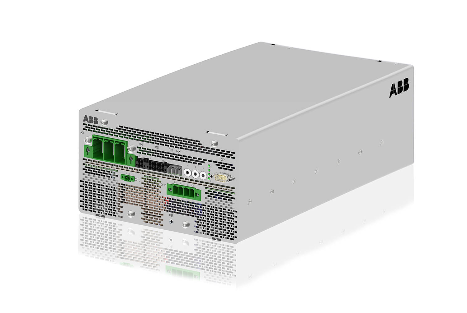
ABB is launching a next generation battery charger based on silicon carbide (SiC) power semicon­ductors for use in all rail applications. Train batteries provide power for critical systems such as control and lighting. The new compact battery charger of the series, BORD­LINE® BC, complements ABB`s large stand-alone auxiliary converter product family and is compatible with all standard train battery voltages.

With a footprint of 360 x 220 mm – the size of a shoebox – it is about 10 times smaller and has a weight reduction of 80 percent compared to previous generations. The new device excels with a high power density of 1 kW per liter and per kg, an improvement from previous generations by a factor of 15.


SiC Silicon carbide infographie ABB batterie chargeur

Modern trains have varying requirements for power electronics components. In local transportation, such as trams, the components need to be as lightweight as possible to improve overall system energy efficiency. The need in long-distance and high-speed transportation is for compact and powerful, yet reliable devices.

The BORDLINE BC battery charger employs ABB’s well proven modular platform design while incorporating SiC technology for the first time. SiC power semiconductor technology enables a power density and performance not possible with conventional silicon (Si) power semiconductors due to its conductivity characteristics. ­Mastering­­­ SiC technology translates into dramatically reduced size, weight, and cooling requirements, and increased system efficiency, all critical factors for rail operators.

“The new battery charger leverages all the benefits available from SiC and soft switching technologies to allow for a new performance level of power electronics in railway,” said Sami Atiya, president of ABB’s Discrete Automation and Motion division. “ABB has a long history of providing innovative and energy-efficient technologies to the rail industry and we will continue innovating for the transportation sector, a key growth area in our Next Level strategy.”

The new high-speed trains by Stadler operated by the Swiss Federal Railways (SBB) on the new transalpine Gotthard base tunnel route between Zurich and Milan will be equipped with this groundbreaking technology.
abbbatterycharger_highres

ABB (www.abb.com) is a leading global technology company in power and automation that enables utility, industry, and transport and infrastructure customers to improve their performance while lowering environmental impact. The ABB Group of companies operates in roughly 100 countries and employs about 135,000 people.

Technological background information:

SiC power semiconductor technology offers significant advantages over traditional silicon-based devices in power applications requiring low losses, high frequency switching and/or high temperature environments. For example, the dielectric strength voltage of SiC is about 10 times greater than that of Si. Low losses are critical to the performance ratio and SiC technology can reduce the power loss by up to a factor of five. High frequency switching can be increased from the conventional technology level with a range of 10 to 20 kHz by a factor of 10.

source

ON Semiconductor Corporation and Fairchild Semiconductor International, Inc. jointly announced today that ON Semiconductor has successfully completed its previously announced $2.4 billion cash acquisition of Fairchild.

“The acquisition of Fairchild is a transformative step in our quest to become the premier supplier of power management and analog semiconductor solutions for a wide range of applications and end-markets,” said Keith Jackson, president and CEO of ON Semiconductor. “Fairchild provides us a platform to aggressively expand our profitability in a highly fragmented industry. With the addition of Fairchild, our industry leading cost structure has further improved in a significant manner and we are now well positioned to generate substantial shareholder value as we integrate operations of the two companies.”

On September 16, 2016, ON Semiconductor received confirmation that clearance related to the completion of its proposed acquisition of Fairchild from the Ministry of Commerce in the People’s Republic of China had been obtained and that ON Semiconductor was entitled to close the transactions under PRC law. As such, the conditions to the acquisition of Fairchild relating to the termination or expiration of required waiting periods, and receipt of required approvals, under applicable antitrust laws were fully satisfied and ON Semiconductor’s tender offer to purchase all of the outstanding shares of common stock of Fairchild for $20.00 per share in cash (the “Offer”) expired as scheduled one minute following 11:59 p.m., New York City time, on September 16, 2016 and was not extended.

Computershare Trust Company, N.A., the depositary for the Offer, advised ON Semiconductor that at the time of the expiration of the Offer, approximately 87,979,761 shares of common stock of Fairchild (not including 7,327,977 shares tendered by notice of guaranteed delivery for which shares have not yet been delivered) were validly tendered and not properly withdrawn pursuant to the Offer, representing approximately 76.6% of the outstanding shares of common stock of Fairchild. In accordance with the terms of the Offer and the merger agreement, all such shares (and any additional shares tendered by guaranteed delivery unless actual delivery does not occur) were irrevocably accepted for payment, and paid for, earlier today.

Immediately following the payment for the tendered shares, ON Semiconductor and Fairchild completed the acquisition of Fairchild by merging it with a wholly owned subsidiary of ON Semiconductor pursuant to which all remaining Fairchild shares (other than shares directly owned by ON Semiconductor or Fairchild or their respective subsidiaries and shares held by stockholders that are entitled to and properly demand appraisal of such shares under Delaware law) were converted into the right to receive $20.00 per share in cash, without interest and less applicable withholding taxes – the same price that was paid in the tender offer. As a result of the Offer and the merger, Fairchild ceased to be a publicly traded company, its common stock will no longer be listed on NASDAQ, and Fairchild became a wholly owned subsidiary of ON Semiconductor.

The acquisition is expected to be accretive on a GAAP EPS basis in the second half of 2017 and immediately accretive on a non-GAAP basis. ON Semiconductor expects to achieve annual cost savings run rate of $160 million by the end of 2017, $200 million by the end of 2018, and $225 million by the end of 2019. The cost savings targets are based on Fairchild’s 2015 annual results.

ON Semiconductor today also announced a new organizational structure, which reflects the evolution over the years of ON Semiconductor’s product portfolio to highly differentiated power management, imaging, and analog solutions from standard products. The new organization is comprised of three reporting units – Power Solutions Group, headed by Bill Hall, Analog Solutions Group, headed by Bob Klosterboer, and Image Sensor Group, headed by Taner Ozcelik. The operations of System Solutions Group have been absorbed in the three reporting units.

Source

VisIC Technologies, Ltd. Is announcing the launch of a new product, offered in a smaller package with bottom side cooling, an on resistance (RDS(ON)) rating of 0.080Ω, and a reduced external components requirement using a simplified driving scheme.

This new 650V GaN Power Switch is a member of the ALL-Switch family designed for bridge converters in motor drives, power supplies, chargers, UPS, Inverters and other circuits requiring high efficiency and currents up to 12A.

VisIC Technology’s designs operate with lower gate charge and capacitance than competitive products while providing the benefits of low RDS(ON). Offered in low inductance packaging, the ALL-Switch family is able to deliver high efficiency. For comparison, ALL-Switch’s switching losses are 3-5 times lower than comparable SIC MOSFET transistors operating at the same frequency.

The V80N65B answers the need expressed by many of VisIC’s customers for a bottom- side cooled package in their designs after they have experienced ALL-Switch’s low switching losses.

The V80N65B Bottom-side cooled power switch supplements VisIC’s, existing ALL Switch top-side cooled product line of 650V GaN devices: The V22N65A, V22S65A, and V18G65A.

EpiGaN, the leading European supplier of commercial 150mm- and 200mm- GaN-on-Silicon epi-wafers for 600V HEMT (High Electron Mobility Transistor) power and RF (Radio Frequency) devices, announces that the Brussels/Beijing-based European private equity fund ACAPITAL has joined the initial investors in EpiGaN to fund the company’s expansion in particular to Asian markets.
EpiGaN,operating out of Hasselt, Belgium, is a key global player in developing and delivering GaN-on-Si and GaN-on-SiC (Silicon Carbide) material solutions worldwide. Gallium Nitride, the most important semiconductor after Silicon, started to revolutionize the energy sector by enabling significant energy loss reduction in power handling, smaller and lighter systems, such as for example for consumer power supplies, photovoltaic inverters, industrial sensors and more generally all products linked with IoT. EpiGaN offers innovative and unique solutions for epitaxial GaN layer structures on 150 mm and 200mm Si substrates in particular with its in-situ SiN (Silicon Nitride) passivation, enabling more robust high-performance devices. EpiGaN’s product portfolio covers state-of-the-art solutions for low-loss power switching, Radiofrequency/Mobile communication power and sensor applications.


“We believe ACAPITAL is the right partner to support the expansion of our business activities into Asia, where we see great opportunities right now”

said EpiGaN co-founder and CEO Dr Marianne Germain. “Our initial investors stay in place to support the continuous growth of the company.” EpiGaN was founded in 2010 by Drs Marianne Germain (CEO), Joff Derluyn (CTO) and Stefan Degroote (COO), as a spin-off from renowned Belgian micro- and nano-electronics research center imec.

Andre Loesekrug-Pietri, founder and managing partner of ACAPITAL commented: “We are very pleased to support the growth of EpiGaN and to join its board of directors. EpiGaN has developed a unique expertise in the gallium-nitride-on-silicon technology for semiconductors, which will allow to build the next generation of energy-efficient devices. Applications are massive: power-electronics, internet of things, smart grid applications, mobile communications and electric mobility: most areas linked with Industry 4.0 and Energy Transition, which are core investment areas for ACAPITAL.” He added : “EpiGaN is uniquely positioned to grasp a significant share of these high-growth markets. We look forward to help scale EpiGaN internationally and in Asia and China in particular, the largest market in the world.”

TDK Corporation and Toshiba Corporation have agreed to establish a joint venture , TDK Automotive Technologies Corporation, that will engage in the development, manufacture and sales of automotive inverters for hybrid vehicles, plug-in hybrid vehicles and electric vehicles.

A Joint venture for Automotive inverters

Many countries propose to impose more stringent regulation of automobile exhaust emissions in 2020 and after, in an effort to prevent air pollution and global warming. This trend to stricter regulation is expected to greatly affect the global automobile market, contributing to an increase in demand for hybrid and plug-in hybrid vehicles in the global market and greatly increased use of electric, fuel-cell, and other eco-friendly vehicles.

Under such market conditions, TDK is currently strengthening its energy unit[1] business, which mainly consists of hardware in power conversion for hybrid, plug-in hybrid, and electric vehicles, as well as software that controls such hardware as strategic growth products in the medium to long term. TDK offers a lineup of products, such as DC-DC converters, on board chargers and wireless power transfer systems that are currently being developed. The DC-DC converter in particular utilizes the magnetic material technologies that are the strength of TDK. They are one of the smallest in the industry and offer high efficiency and other product advantages that have won global recognition and a delivery record of more than 2.5 million units in aggregate.

Upon the establishment of the JV with Toshiba as described above, TDK’s energy unit business is expected to expand tremendously, as the addition of automotive inverters to TDK’s product lineup will broaden its product range and enable to meet diverse customer demand.

Toshiba develops technologies to meet automobile manufacturers’ requirements for low fuel consumption that combine advanced capabilities in automotive inverters with 120 years of cumulative know-how in motors. By integrating power semiconductor modules, Toshiba’s inverters secure high levels of heat dissipation in a short time, and also contribute to downsizing that reduces space requirements. Toshiba aims to strengthen its competitiveness in the growing market for automotive inverters and motors by combining its highly efficient automotive motors with automotive inverters developed by the JV and DC-DC converters developed by TDK, and proposing them as a system for hybrid and electric vehicles.


TDK Automotive Technologies profile:

1) Company name TDK Automotive Technologies Corporation
2) Address of the Head Office 3-9-1 Shibaura, Minato-ku, Tokyo, Japan  (within TDK Corporation)
3) Address of the business premises 2-15-7, Higashiohwada, Ichikawa-shi, Chiba, Japan (within TDK Technical Center)

2000 Nao, Mie-gun Asahi-cho, Mie, Japan

4) Main business Development, manufacturing and sales of automotive inverters
5) Stated capital 400 million yen
6) Ratio of capital contribution TDK: 75%; Toshiba: 25%
7) Date of establishment October 1, 2016 (scheduled)
8) Date of business start December 1, 2016 (scheduled)

ON Semiconductor Corporation announced today that the U.S. Federal Trade Commission has accepted a proposed consent order for public comment and has terminated the Hart-Scott-Rodino waiting period applicable to ON Semiconductor’s proposed acquisition of Fairchild Semiconductor International, Inc. Under the proposed consent order and in order to satisfy the FTC’s remaining concerns, prior to the closing of the acquisition of Fairchild, the FTC required that ON Semiconductor dispose of its planar insulated gate bipolar transistor (“Ignition IGBT”) business, which business generated less than $25 million in revenue during fiscal year 2015. In satisfaction of this requirement, ON Semiconductor announced today that it has entered into a definitive agreement with respect to the divestiture of the Ignition IGBT business to Littelfuse, Inc. and has also entered into a separate definitive agreement with Littelfuse to sell its transient voltage suppression (“TVS”) diode and switching thyristor product lines, for a combined $104 million in cash. No manufacturing assets will be transferred by ON Semiconductor in connection with the divestiture of the Ignition IGBT business or the sale of the TVS and thyristor businesses, and both asset sales are expected to close on August 29, 2016.

ON Semiconductor acquisitions conditions Fairchild Littelfuse

The completion of ON Semiconductor’s previously announced tender offer (the “Offer”) to purchase all of the outstanding shares of common stock of Fairchild for $20.00 per share in cash remains subject to certain customary terms and conditions set forth in the Offer to Purchase, dated December 4, 2015, as amended (the “Offer to Purchase”), and other related materials by which the Offer is being made.

The condition to the Offer relating to the termination or expiration of required waiting periods under the HSR Act has been satisfied. The proposed FTC consent order is subject to public comment for 30 days and to final approval by the FTC, although this will not affect the parties’ ability to close the transaction when all other conditions to closing have been satisfied.

Littelfuse, Inc., announced it has entered into definitive agreements to acquire the product portfolio of transient voltage suppression (“TVS”) diodes, switching thyristors and insulated gate bipolar transistors (“IGBT”) for automotive ignition applications from ON Semiconductor Corporation for a combined purchase price of $104 million. This portfolio has annualized sales of approximately $55 million. The transactions are expected to close in late August, 2016.

“The acquisition of this portfolio aligns with our strategy to expand in power semiconductor applications as well as increase our presence in the automotive electronics market,”

said Ian Highley, senior vice president and general manager, semiconductor products and chief technology officer for Littelfuse. “These products have strong synergies with our existing circuit protection business, will strengthen our channel partnerships and customer engagement, and expand our power semiconductor portfolio.”

Littelfuse also plans to invest approximately $30 million in its semiconductor fabrication locations to enhance its production capabilities, add significant capacity to its China fabrication facility and transfer the production of the acquired portfolio. The transfers will occur over the next few years, as the company works with customers on their timing and requirements. The expected productivity gains from this investment will drive long term profitable growth across the company’s semiconductor business.

“Once we complete the transfer of these products, we expect this acquisition to have EBITDA margins of more than 30 percent,” added Meenal Sethna, executive vice president and chief financial officer. “Including amortization, interest and integration expenses, we expect the earnings per diluted share impact of this acquisition to be neutral in 2016, and accretive in 2017 and beyond.”

Wachtell, Lipton, Rosen and Katz is acting as legal advisor to Littelfuse.

About Littelfuse

Founded in 1927, Littelfuse is the world leader in circuit protection with growing global platforms in power control and sensing. The company serves customers in the electronics, automotive and industrial markets with technologies including fuses, semiconductors, polymers, ceramics, relays and sensors. Littelfuse has over 10,000 employees in more than 40 locations throughout the Americas, Europe and Asia. For more information, please visit the Littelfuse website: Littelfuse.com.

Source

Dialog Semiconductor, a provider of power management, AC/DC power conversion, solid state lighting (SSL) and Bluetooth® low energy technology, today announced and is demonstrating its first gallium nitride (GaN) power IC product offering, using Taiwan Semiconductor Manufacturing Corporation’s (TSMCs) 650 Volt GaN-on-Silicon process technology.

The DA8801 together with Dialog’s patented digital Rapid Charge™ power conversion controllers will enable more efficient, smaller, and higher power density adapters compared to traditional Silicon field-effect transistor (FET) based designs today. Dialog is initially targeting the fast charging smartphone and computing adapter segment with its GaN solutions, where it already enjoys more than 70 percent market share with its power conversion controllers.

“The exceptional performance of GaN transistors allows customers to deliver more efficient and compact power adapter designs that meet today’s market demands,”

said Mark Tyndall, SVP Corporate Development and Strategy, Dialog Semiconductor. “Following our success in BCD-based power management ICs (PMICs), as an early GaN innovator, Dialog once again leads the commercialization of a new power technology into high-volume consumer applications.”

GaN technology offers the world’s fastest transistors, which are the core of high-frequency and ultra-efficient power conversion. Dialog’s DA8801 half-bridge integrates building blocks, such as gate drives and level shifting circuits, with 650V power switches to deliver an optimized solution that reduces power losses by up to 50 percent, with up to 94 percent power efficiency. The product allows for a seamless implementation of GaN, avoiding complex circuitry, needed to drive discrete GaN power switches.

The new technology allows a reduction in the size of power electronics by up to 50 percent, enabling a typical 45 Watt adapter design today to fit into a 25 Watt or smaller form factor. This reduction in size will enable true universal chargers for mobile devices.

“As Dialog’s strategic foundry partner for power management ICs for many years, we are delighted to have expanded our relationship to collaborate closely in bringing our GaN process to the mainstream consumer market for high volume applications,” said Maria Marced, President of TSMC Europe. “Dialog’s first GaN product delivers on the promise of GaN while bringing the integration to a higher level.”

The DA8801 will be available in sample quantities in Q4 2016. More information on the DA8801 can be found here:  http://www.dialog-semiconductor.com/products/DA8801

Watch the DA8801 GaN video here: https://youtu.be/O9ks-j0R6PA

Source

Mitsubishi Electric Corporation  announced today the launch of a new transfer-mold power semiconductor model in its lineup of Super-mini Dual-In-line Package Intelligent Power Modules (DIPIPMTM), embedded with Silicon Carbide Metal-Oxide-Semiconductor Field-Effect Transistors (SiC-MOSFET). It will launch on August 17.

Product Features

1) Top class low power consumption in the home appliance market

SiC-MOSFET reduces power consumption by about 70 percent compared with Mitsubishi Electric’s existing Super-mini DIPIPM, and contributes to an overall reduction in air conditioner power consumption
2) Simplified inverter system design

Footprint and pin configurations are compatible with Mitsubishi Electric’s existing Super mini DIPIPM Ver.6, PSSxxS92x6series,etc.
Designed with a high threshold voltage, SiC-MOSFET does not require a negative bias circuit, allowing simplification of the system design
Fewer external components due to use of embedded bootstrap diode with current-limiting resistor

Sales Schedule

Model Specification Shipment
PSF15S92F6 15A/600V August 17, 2016

source

STMicroelectronics has introduced a portfolio of TO-220 FullPAK (TO-220FP) wide creepage power transistors, including the world’s first 1500V super-junction MOSFET in this new important arcing-resistant package.STMicroelectronics Introduces New Super-Junction MOSFETs including World’s First 1500V Device in TO-220FP Wide Creepage Package

The TO-220FP wide creepage package is ideal for the power transistors of open-frame power supplies commonly used in equipment such as television sets and PCs, which are vulnerable to surface contamination by dust and particles that can cause high-voltage arcing between transistor terminals. The new package’s extended lead spacing of 4.25mm eliminates the special potting, lead forming, sleeving, or sealing needed to prevent the arcing when using conventional packages with 2.54mm lead spacing. Power-supply manufacturers can now meet applicable safety standards and minimize field failures without applying these additional processes, thereby simplifying manufacturing and enhancing productivity.

While providing superior arcing resistance, TO-220FP wide creepage retains the outstanding electrical properties of the popular TO-220FP. Moreover, similar outer dimensions help streamline design-in and ensure compatibility with established assembly processes.

ST developed the TO-220FP wide creepage package by collaborating with its customer SoluM, a leading power manufacturer based in Korea. SoluM is using the superior package to create new power solutions that are more robust and cost-effective than competing products.

ST is currently ramping up production of TO-220FP wide creepage power transistors to support a major global television manufacturer. The product portfolio includes four fully qualified 600V low-RDS(ON) MDmesh™ M2 MOSFETs with current ratings from 8A to 34A. The 1500V STFH12N150K5 and 1200V STFH12N120K5, MDmesh K5 devices, will be qualified by the end of Q3 2016.

Taiyo Yuden and GE Ventures announced today that they entered into a license agreement for an intellectual property (IP) to fabricate substrates embedded with electronic circuits in late 2014. With this technology transfer, Taiyo Yuden and GE will construct a joint development framework toward the commercialization of next-generation wirebondless, embedded electronics circuits. Taiyo Yuden will develop Si-, SiC- and GaN-based wirebondless embedded electronics circuits with the technology and the patent licenses provided by GE Ventures Licensing. Embedded electronic packaging technologies provide significantly improved electrical performance (for example, reduced parasitics), can increase functional density of the electronics circuits by more than a third, and can increase efficiency by over 10%.

GE General Electric Shinko Power overlay POL power module packaging

Extract from “Packaging Challenges and Solutions
for Silicon Carbide Power Electronics” – ECTC 2012 – Ljubisa Stevanovic

“We are extremely pleased to have Taiyo Yuden as an embedded electronics partner,” said Pat Patnode, President of Licensing at GE Ventures.

“The strong demand for high performance electronics circuits continues to drive advance research, and GE is excited to partner with Taiyo Yuden to bring wirebondless embedded packaging solutions to the next generation of electronics.” These embedded electronics circuits can be built into higher level power assemblies and systems for a wide variety of applications.

“Taiyo Yuden will target power devices, Internet of Things (IoT), and wearable applications with this GE Power Overlay (POL) technology. “

This technology will allow additional new application opportunities leveraging the strength of Taiyo Yuden’s current packaging and assembly technology capability and experience.” Said, Hiroshi Kishi, Operating Officer, Research and Development Laboratory. GE Ventures accelerates innovation and growth for partners by providing access to GE technologies and inventions through licensing and joint development partnerships.

Source

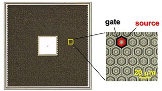
Toyoda Gosei Co., Ltd. has developed the world’s first 1.2 kV class power semiconductor device (a general term for power rectifier diodes, switching transistors, etc.) chip capable of large current operation exceeding 20 A. This was done using gallium nitride (GaN), a key material in blue LEDs, which has superior physical properties including the ability to withstand high voltages.

Toyoda gosei GaN 1.2kV hemt power electronics

Using the crystal growth technology we have cultivated since 1986 in the development and production of blue LEDs, we began research for the development of device technology for power semiconductors using GaN in 2010. Previously, low loss MOSFETs (a type of transistor used in power devices*) of the 1.2 kV class were fabricated on GaN substrates and then empirically tested. We have now established wiring technology for the parallel operation of elements, successfully passing an electrical current exceeding 20 A in a vertical GaN transistor with a 1.5 mm square chip size. This is the first time that has ever been achieved, according to a Toyoda Gosei survey.

The developed technology are applied to circuits for the power controllers on hybrid vehicles that handle large amounts of power, and to power converters such as those in solar power generation, which promises significant contributions in making these devices more compact and efficient. We will continue research to increase the current capacity and test reliability with the aim of developing commercial applications by about 2018-2020 in collaboration with semiconductor and electronics manufacturers.

Source