Tag Archive for: Device

Electric car makers are to become Smart-grid system makers

In June 2015, PointThePower.com made an analysis of electric car manufacturing business and the link that will be made with energy grid and energy storage. This analysis is now becoming true. After Tesla, Daimler and Audi, it’s now Nissan’s turn to announce that they will use second-hand batteries for home energy storage.

So if you missed the analysis, here is a synthesis: Back in time, Alstom, Siemens, GE, Mitsubishi Electric and few other huge companies became both electric transport system makers and energy production or storage system makers. This happened because the core competency to target was Power electronics, and they mastered the topic. They either started with transportation systems to come to energy, or the other way round.

Now that the car market is becoming electric, and that energy production is coming down to consumer level, the same thing is happening. Car makers master “consumer power range” electric systems. So, you will soon see electric car makers becoming full energy supply-chain players, at lower power levels compared to Alstom and Siemens.

We performed this analysis almost one year ago: It’s still available in full here.

For more info about Nissan/Eaton solution, just read below:

Nissan and Eaton release “xStorage”

Nissan and Eaton, have joined forces to unveil a new residential energy storage unit. Available to pre-order from September 2016, the “xStorage” solution will give consumers possibility to control how and when they use energy in their own homes.

Connected to residential power supply or renewable energy sources such as solar panels, the unit can charge up when renewable energy is available or energy is cheaper (e.g. during the night) and release that stored energy when demand and costs are high.

The home energy storage system also provides a back-up solution to consumers, ensuring that the lights never go out. Moreover, customers can sell stored energy back to the grid when demand and costs are high.
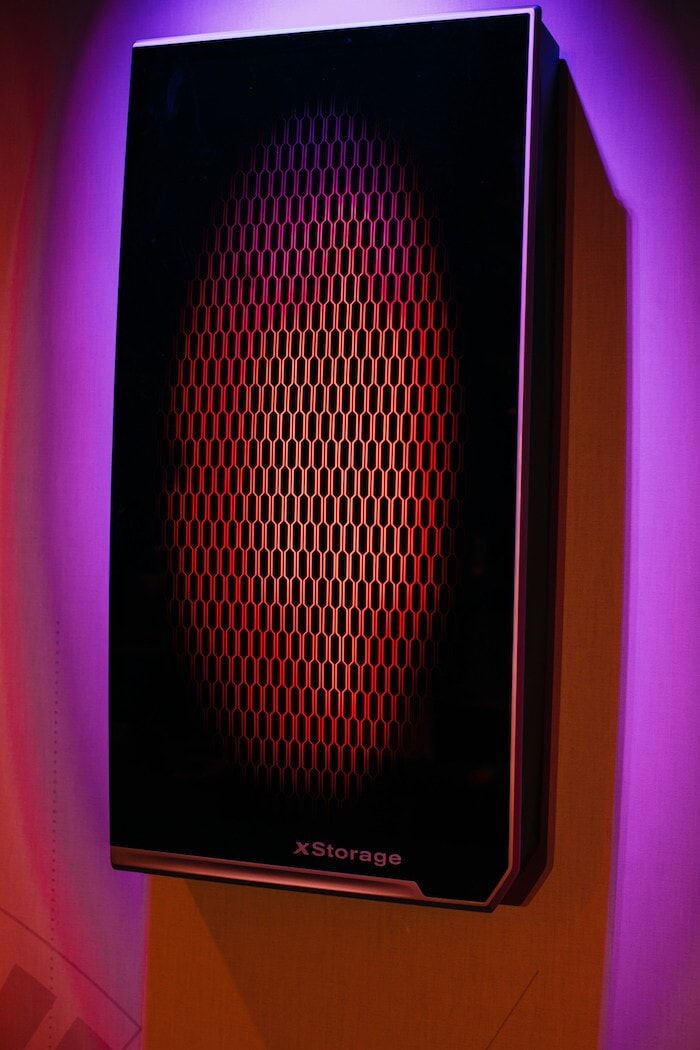
 

Nissan Eaton Xstorage home storage battery

It’s providing a sustainable “second life” for Nissan’s electric vehicle (EV) batteries after their first life in cars is over, the new unit is powered by twelve Nissan EV battery modules and has the potential to revolutionize the way people manage energy usage in their own home, providing added flexibility and multiple cost savings.

“The collaborative development between Eaton and Nissan enabled us to optimize development and production costs and deliver a well-integrated offer to consumers. Our system will be provided to end-users completely ready to use, with all required elements including cabling and installation by a certified professional, at a starting price of €4,000 (£3200) for 4.2KWh nominal. Our policy is to avoid hidden extra costs and achieve a lower total cost of ownership than other major offers already announced.”

, said Cyrille Brisson, VP Marketing at Eaton Electrical EMEA.

The new xStorage system unveiled today marks the start of a longer-term commitment by Nissan and Eaton to widen the portfolio of energy storage solutions available to both private and commercial customers. Nissan and Eaton expect to sell more than 100,000 xStorage units within the next five years as the consumer appetite for this type of technology continues to grow.

Source

Ascatron develops power semiconductors based on Silicon Carbide (SiC) that radically reduce losses in electrical transformers. Ascatron focuses on high voltage applications where the energy savings will be very large by using SiC.

Ascatron SiC Silicon Carbide diode package 3DSiC high temperature

1200V SiC power diode for high temperature operation at 250°C

They have now completed the A-round financing intended for the final development of its first own SiC semiconductor products. The total of 4 M€ is shared between 3 M€ in equity capital, and
1 M€ in an innovation grant.

“We have started to implement our advanced material technology in a production equipment for SiC epitaxy”, says Adolf Schöner, CTO of Ascatron.

“The next step is to optimize our device design and outsource the remaining manufacturing of the chip to a foundry with capacity for volume production”.

The A-round investors are from Italy and China, including the four venture capital investors Quadrivio, Como Venture, Rise Leader Investment and InteBridge Technology, together with the equipment producer LPE. The grant comes from the European Institute of Innovation and Technology (EIT) through KIC InnoEnergy. KIC supports innovation projects in the field of sustainable energy.

“Our investors have a good mix of understanding both the advanced material technology needed for high performance SiC power devices, and how to address volume markets for semiconductors”

says Christian Vieider, CEO of Ascatron. “40% of the market for power electronic components is in China, and there is a lot of interest in SiC for energy saving”.

About Ascatron

Ascatron develops next generation Silicon Carbide (SiC) power semiconductors radically reducing electrical conversion losses. Target applications are process industry, data center, traction, wind power and grid transformers. With the 3DSiC® technology Ascatron makes doped device structures based on epitaxy, enabling device performance with very low losses and capacity to handle very high voltage. Ascatron started the operation in 2011 as a spin-out from the Swedish R&D institute Acreo, and has 10 employees in Sweden. www.ascatron.com

Toshiba Electronics Europe is set to announce the development of its next generation of superjunction (SJ) deep trench semiconductor technology for high-efficient power MOSFETs.  Devices based on the new DTMOS V process operate with lower EMI noise and reduced on resistance (RDS(ON)) compared to previous DTMOS IV MOSFETs.


As with the previous DTMOS IV semiconductor technology, DTMOS V is based on a single epitaxial process involving ‘deep trench etching’ followed by P-type epitaxial growth.  The deep trench filling process results in a narrowing of cell pitch and a lowering of RDS(ON) when compared with more conventional planar processes. Toshiba’s deep trench process allows an improved thermal coefficient of RDS(ON) compared to conventional super junction MOSFETs using multi epitaxial growth process.

With DTMOS V, Toshiba has been able to reduce RDS(ON) of the DPAK TK290P60Y by up to 17% compared with the lowest RDS(ON)available from the TK12P60W DTMOS IV MOSFET. The company has also further optimised the trade-off between switching performance and EMI noise.

DTMOS V MOSFETs will simplify the design and improve the performance of power conversion applications, including switching power supplies, power factor correction (PFC) designs, LED lighting and other AC/DC applications. The first MOSFETs based on the fifth generation process will offer ratings of 600V and 650V and be supplied in DPAK (TO-252) and TO-220SIS (smart isolation) packaging. Maximum ON resistance ratings will range from just 0.29Ω to 0.56Ω.

Exagan, a start-up manufacturing gallium nitride (GaN) semiconductor technology for power electronics has begun a strategic partnership to develop and commercialize GaN-on-silicon products withHIREX Engineering, a company of Alter Technology Group (TÜV NORD GROUP’s Aerospace and Electronics Business Unit). The partnership’s goal is to establish the reliability and quality of GaN-on-silicon power devices.
Exagan will work closely with HIREX Engineering, a leader in reliability testing and qualification of ICs and discrete semiconductors for aerospace and industrial high-reliability applications. HIREX Engineering is located near Toulouse, France. Together, the companies will test and qualify Exagan’s G-FET™ products, which are fabricated with standard 200-mm silicon processing and proprietary G-Stack™ technology. G-FETs are used in making smaller, more efficient power converters that have a broad range of applications (plug-in hybrid and full-electric vehicles, solar energy, industrial applications, or charging of all mobile electronic devices).

“This dynamic partnership will help to propel GaN market development by pioneering test methodologies and measurement processes that make it easier for makers of electrical converters to implement GaN in improving their products,” said Frédéric Dupont, president and CEO of Exagan.

“This timing is perfect to combine Exagan’s strengths with those of the top European specialist in high-reliability testing. GaN technology has matured to deliver the high performance of SiC (silicon carbide) devices at silicon ICs’ price and quality levels, and our key markets are ready for this next-generation solution.”

“Through its participation, HIREX Engineering will expand its expertise and business portfolio to include advanced power GaN technology and the end products it enables. We hope to establish robust and easy-to-reference product parameters for GaN that will allow fast integration in electrical converters,” said Luis Gomez, Alter Technology Group CEO.

“We are confident that GaN’s bulletproof reliability will present remarkable advantages in the fast-growing power electronics market,” said Dr. Guido Rettig, TÜV NORD GROUP CEO.

Infineon Technologies AG has unveiled a revolutionary silicon carbide (SiC) MOSFET technology.

“For more than twenty years, Infineon has been at the forefront of developing SiC solutions which address demands for energy savings, size reduction, system integration and improved reliability,” said Dr. Helmut Gassel, President of Infineon’s Industrial Power Control Division. “Infineon has manufactured millions of products containing SiC devices, while our Schottky diode and J-FET technologies have allowed designers to achieve power density and performance not possible with conventional silicon. The strategy has now taken a significant step forward encompassing power MOSFETs that raise the benefits available from SiC technology to a new level, which has never before been possible.”

The new 1200 V SiC MOSFETs have been optimized to combine reliability with performance. They operate with ‘benchmark’ dynamic losses that are an order of magnitude lower than 1200 V silicon (Si) IGBTs. This initially supports system improvements in applications such as photovoltaic inverters, uninterruptible power supplies (UPS) or charger/storage systems, while later configurations will also extend support to industrial drives.

The MOSFETs are fully compatible with the +15 V/-5 V voltages typically used to drive IGBTs. They combine a benchmark threshold voltage rating (V th) of 4 V with short-circuit robustness required by the target applications and fully controllable dv/dt characteristics. Key benefits over Si IGBT alternatives include temperature-independent switching losses and threshold-voltage-free on-state characteristics.

The new MOSFETs are based on a state-of-the-art trench semiconductor process and represent the latest evolution of Infineon’s comprehensive family of CoolSiC technologies. This family includes Schottky diodes and 1200 V J-FET devices and a range of hybrid solutions that integrate a Si IGBT and SiC diode in a module device.

The first discrete 1200 V CoolSiC MOSFETs feature on-resistance (R DS(ON)) ratings of just 45 mΩ. They will be available in 3-pin and 4-pin TO-247 packages targeted at photovoltaic inverters, UPS, battery charging and energy storage applications. Both devices are ready for use in synchronous rectification schemes thanks to the integration of a commutation robust body diode operating with nearly zero reverse recovery losses. The 4-pin package incorporates an additional (Kelvin) connection to the source, which is used as a reference potential for the gate driving voltage. By eliminating the effect of voltage drops due to source inductance, this further reduces switching losses, especially at higher switching frequencies.

Infineon has also announced 1200 V ‘Easy1B’ half-bridge and booster modules based on the SiC MOSFET technology. Combining PressFIT connections with a good thermal interface, low stray inductance and robust design, each module is available with R DS(ON)rating options of 11 mΩ and 23 mΩ.

Availability

Infineon will start sampling for target applications in the second half of 2016, with volume production planned for 2017. More information is available at www.infineon.com/coolSiC.

Texas Instruments today announced the availability of 600-V gallium nitride (GaN) 70-mΩ field-effect transistor (FET) power-stage engineering samples, making TI the first and only semiconductor manufacturer to publicly offer a high-voltage driver-integrated GaN solution. The new 12-A LMG3410 power stage coupled with TI’s analog and digital power-conversion controllers enables designers to create smaller, more efficient and higher-performing designs compared to silicon FET-based solutions. These benefits are especially important in isolated high-voltage industrial, telecom, enterprise computing and renewable energy applications.

“With over 3 million hours of reliability testing, the LMG3410 gives power designers the confidence to realize the potential of GaN and to rethink their power architecture and systems in ways not feasible before,” said Steve Lambouses, TI vice president of high-voltage power solutions. “Expanding on TI’s reputation for manufacturing capability and extensive system-design expertise, the new power stage is a significant step for the GaN market.”

With its integrated driver and features such as zero reverse-recovery current, the LMG3410 provides reliable performance, especially in hard-switching applications where it can dramatically reduce switching losses by as much as 80 percent. Unlike stand-alone GaN FETs, the easy-to-use LMG3410 integrates built-in intelligence for temperature, current and undervoltage lockout (UVLO) fault protection.

Proven manufacturing and packaging expertise
The LMG3410 is the first semiconductor integrated circuit (IC) to include GaN FETs manufactured by TI. Building on years of expertise in manufacturing and process technologies, TI creates its GaN devices in a silicon-compatible factory and qualifies them with practices that are beyond the typical Joint Electron Device Engineering Council (JEDEC) standards to ensure the reliability and robustness of GaN for demanding use cases. Easy-to-use packaging will help increase the adoption of GaN power designs in applications such as power factor controller (PFC) AC/DC converters, high-voltage DC bus converters and photovoltaic (PV) inverters.

Key features and benefits of the LMG3410

  • Double the power density. The 600-V power stage delivers 50 percent lower power losses in a totem-pole PFC compared with state-of-the-art silicon-based boost power-factor converters. The reduced bill of materials (BOM) count and higher efficiency enable a reduction in power-supply size of as much as 50 percent.
  • Reduced packaging parasitic inductance. The new device’s 8-mm-by-8-mm quad flat no-lead (QFN) package decreases power loss, component voltage stress and electromagnetic interference (EMI) compared to discrete GaN solutions.
  • Enables new topologies. GaN’s zero reverse-recovery charge benefits new switching topologies, including totem-pole PFC and LLC topologies to increase power density and efficiency.

Expanding the GaN ecosystem
To support designers who are taking advantage of GaN technology in their power designs, TI is also introducing new products to expand its GaN ecosystem. The LMG5200POLEVM-10, a 48-V to 1-V point-of-load (POL) evaluation module, will include the new TPS53632G GaN FET controller, paired with the 80-V LMG5200 GaN FET power stage. The solution allows for efficiency as high as 92 percent in industrial, telecom and datacom applications.

Availability and pricing
TI will offer a development kit that includes a half-bridge daughtercard and four LMG3410 IC samples. A second kit contains a system-level evaluation motherboard. When used together, these two kits enable immediate bench testing and design. The two development kits are available for purchase now in the TI store and are priced at $299.00 and $199.00, respectively.


For more details, see www.ti.com/lmg3410-pr.

Freebird Semiconductor, a US manufacturer of high reliability GaN HEMTs, and Efficient Power Conversion (EPC) have entered into an agreement to develop products for high reliability, space and harsh environment applications based on EPC’s eGaN power transistors and ICs.

Simon Wainwright, president and CEO of Freebird Semiconductor said: “GaN technology will permit space applications to use the latest in high performance semiconductor material, whereas using silicon-based components in these applications produces systems that are behind the latest performance curves.”

“The superior conductivity and switching characteristics of GaN devices allow designers to greatly reduce system power losses, size, and weight. Given GaN’s superior state-of-the-art performance, coupled with its demonstrated ability to operate reliably under harsh environmental conditions and high radiation, GaN devices have a very bright future in space applications. We are excited to be supporting Freebird in the development of their GaN-based products,”

noted Alex Lidow, EPC CEO and co-founder.

In addition to collaborating on power systems product development, the two companies will be active in publishing the results of their work and giving joint presentations at professional conferences.

Source

Ideal Power Inc., a developer of innovative power conversion technologies, reported its semiconductor fabricator successfully tested Bi-Directional Bi-Polar Junction TRANsistor (B-TRAN™) silicon dies and test results validate key characteristics of the semiconductor power switch. The test results can be found in the company’s updated B-TRAN White Paper. The results confirm central B-TRAN™ elements and operational modes are consistent with third party device simulations that predict significant performance and efficiency improvements over conventional power switches such as SCRs, IGBTs and MOSFETs.

B-TRAN™ device is a symmetric double-sided structure that presents opportunities for high current density operation at high efficiency.

“This validation of key characteristics of the B-TRAN™ technology is a significant step forward in demonstrating B-TRAN’s ability to improve energy efficiency across a wide range of products and applications,”

said Dr. Richard Blanchard, B-TRAN™ co-inventor and holder of over 200 patents primarily related to power semiconductors including the widely used trench MOSFET.

“The device has tremendous implications for the power industry.”

“These exciting results of the first tested B-TRAN™ structures validate key characteristics of the device and confirm our belief that B-TRANs can be a disruptive new force in many power conversion applications,” said Bill Alexander, CTO of Ideal Power and co-inventor of the B-TRAN™. “The predicted extremely low forward voltage drop and fast, low loss switching of the B-TRAN™ are each approximately ten times better than conventional switches. B-TRAN’s high current density and native bi-directional capability can lead to very high efficiency power control and conversion at very low cost points. We expect these anticipated efficiency improvements to translate to a substantial cost-performance advantage over current generation power semiconductor devices, which opens a multi-billion dollar market opportunity for the B-TRAN™ and is generating licensing inquiries from power semiconductor companies.”

Ideal Power plans to introduce the B-TRAN™ into the rapidly growing IGBT power semiconductor market, estimated to be close to $5 billion in 2015 according to Point The Gap . The next major milestone for commercializing the B-TRAN™ will be testing a fully-packaged device.

Ideal Power believes its new B-TRAN™ technology can potentially address up to 50% of the power semiconductor market as a replacement for older, less efficient power switch technologies such as IGBTs and MOSFETs, as well as the newer gallium nitride (GaN) and silicon carbide (SiC) devices. Potential addressable markets for B-TRAN-based products include very low loss solid-state DC and AC contactors, electric vehicle drivetrains, variable frequency drives, solar photovoltaic inverters, bi-directional energy storage and microgrid power conversion systems, matrix converters and other power conversion products.

Based on third party simulations and testing to date, the Company expects the B-TRAN to deliver 10 to 200 times the cost-performance of current power semiconductor switches, depending on the switch type and configuration, with cost-performance being defined as the combination of device cost and on-state resistance. For a given cost, the B-TRAN™ is expected to have 10 to 200 times lower on-state resistance, while simultaneously having up to 10 times faster switching than other silicon-based switches.

A collaboration between Pi Innovo’s electronics design and development expertise and GaN Systems’ gallium nitride (GaN) semiconductors, offers automakers a pathway to the electrification of auxiliary systems for multi-voltage conventional, hybrid-electric, and pure electric vehicles.

Based on GaN Systems’  technology, gallium nitride devices use GaN-on-silicon base wafers. The company manufactures a range of gallium nitride power transistors for automotive, consumer, datacenter, industrial and solar/wind/smart grid applications.

Pi Innovo has designed and implemented custom motor control electronics to take advantage of the benefits of GaN Systems semiconductors in applications with a range of input voltages from 12V to 300V. This controller design provides a functional starting-point for the development of 48V and above, high-speed motor-driven vehicle systems, and adds to a growing portion of Pi Innovo’s business providing custom electronics solutions across multiple markets.

PI Innovo GaN Systems motor drive for electric vehicle

Following the success of this GaN-based multi-voltage motor controller development project, Pi Innovo is now offering design and development services in support of customers looking to adopt this technology for a wide range of electronics design applications in automotive and adjacent markets. The company is positioned to support customers wanting to develop prototype evaluations to quantify the benefits of GaN technology. Pi Innovo can also provide customized cost effective high volume designs for customers looking to go into production.

“Pi Innovo’s hardware, software and applications engineers worked closely with the GaN Systems team to understand their semiconductor design requirements and to ensure the final controller design maximizes the reduction in size, weight and power consumption benefits that gallium nitride semiconductors provide,”

said Dr. Walter Lucking, CEO of Pi Innovo.

“Working with GaN Systems on this project has been a great experience for our team and we’re looking forward to continuing our close partnership to support our customers on many future designs.”

“Having a technology development partner like Pi Innovo that really understands the intricacies of control electronics design for vehicle applications, is invaluable in supporting the continued adoption of GaN in the electrification of vehicle systems,” said Jim Witham, GaN Systems’ CEO.

Source

Navitas Semiconductor today announced the world’s first Gallium Nitride (GaN) Power ICs, using its proprietary AllGaN™ monolithically-integrated 650V platform. Combining GaN power FETs with GaN logic and drive circuits enables 10x-100x higher switching frequency than existing silicon circuits, making power electronics smaller, lighter and lower cost. A new generation of high frequency, energy efficient converters is being enabled for smartphone and laptop chargers, OLED TVs, LED lighting, solar inverters, wireless charging devices and datacenters.

“Breaking Speed Limits with GaN Power ICs”

“GaN has tremendous potential to displace silicon in the power electronics market given its inherent high-speed, high-efficiency capabilities as a power FET,”

says Dan Kinzer, Navitas CTO & COO.

“Previously, that potential was limited by the lack of equally high performance circuits to drive the GaN FETs quickly and cost effectively. Navitas has solved this remaining challenge to unlock the full potential of the power GaN market. With monolithic integration of GaN drive and logic circuits with GaN power FETs, the industry now has a path to cost-effective, easy-to-use, high-frequency power system designs.”

CEO Gene Sheridan added,

“The last time power electronics experienced a dramatic improvement in density, efficiency and cost was in the late 70s when silicon MOSFETs replaced bipolar transistors, enabling a transition from linear regulators to switching regulators. A 10x improvement in density, 3x reduction in power losses and 3x lower cost resulted a short time thereafter. A similar market disruption is about to occur in which GaN power ICs will enable low-frequency, silicon-based power systems to be replaced by high-frequency GaN with dramatic improvements in density, efficiency and cost. This is an exciting time for the industry.”

About Navitas:

Navitas Semiconductor Inc. is the world’s first and only GaN Power IC company, founded in El Segundo, CA, USA in 2013. Navitas has a strong and growing team of power semiconductor industry experts with a combined 200 years of experience in materials, circuits, applications, systems and marketing, plus a proven record of innovation with over 125 patents among its founders. The proprietary AllGaN™ process design kit monolithically-integrates the highest performance 650V GaN FET and GaN driver capabilities. Navitas GaN Power ICs enable smaller, higher energy efficient and lower cost power for mobile, consumer, enterprise and new energy markets. Over 25 Navitas proprietary patents are granted or pending.

Source

Fairchild has released its first 1200V SiC diode, the FFSH40120ADN. The company says the diode’s combination of superior switching performance, higher reliability and low electromagnetic interference (EMI) make it suitable for next-generation solar inverters, industrial motor controls and welders.

“The combination of market trends and tightening industry standards is driving the need for more energy efficient products and our new 1200V SiC diode is designed specifically to help manufacturers achieve these ever-greater efficiency requirements and with better reliability, ruggedness and cost efficiency,”

said Jin Zhao, VP and general manager of Fairchild’s High Power Industrial division.

“We based this diode on SiC due to the material’s considerable advantages over silicon, and we will add additional SiC-based semiconductors as we build a comprehensive family of SiC solutions,” he added.

The FFSH40120ADN diode is claimed to have the best leakage current performance in its class, leaking far less current than its competitors at temperatures up to 175degC. Other benefits of the new diode include fast switching and no reverse recovery current, which reduces switching losses compared to silicon and results in superior energy efficiency.

The diode’s ability to switch stably over a wide temperature range is another factor contributing to its performance, as is its zero recovery voltage which eliminates voltage overshoots.

Fairchild will demonstrate the performance of the new diode at the upcoming APEC conference, March 20-24 in Long Beach, California.

Source

GaN again: good news?

I remember reading a tribune on TI social blog about how much GaN discussions were exhausting these days. The author said that APEC 2015 was hammering with GaN. We have been talking about GaN over and over. And every year it’s the same thing. 2015 Rap Session at APEC concluded once more that “It’s here, it’s coming. It’s good. We need to use it.” The round-table captivated the audience, as usual, but it leads to the same talks and questions with the same kind of people. I understand it becomes exhausting. It’s too much, even for me. I would like Gallium Nitride devices to be out, used everywhere, and that we start talking about something else, like Diamond or carbon nanotubes. I wish we had passed the curve, and we were at the top of it and we were looking at something else.

But we are not there yet. We will still see a lot of GaN, but I hope and I think that we will see different GaN. Let me explain why such a theory.

Why we will see GaN again at APEC this year

We already have device start-ups and bigger companies working on Gallium Nitride devices. We know the pros and cons. We know a lot about the devices themselves. So why would we still talk about that in 2016 at APEC? I wrote recently an article about why we still cannot find GaN in small power supplies (like Zolt and maybe FinSix). GaN devices will irrigate the market in the near future. You find all the analysis, explanations and some roadmap in the GaN Market Analysis report that we’re going to release next month. But there is still a missing thing: conversion systems (and the specialists that come with it).

And Point The Gap’s belief is that this is the next step for GaN. The step where you see big companies trying to use GaN devices, and where you see a few start-ups developing new types of systems. They work on new topologies, architectures, innovative passive components, PCB design or anything needed to make GaN or SiC deliver their best. This new era has started with FinSix  back when it was still On-Chip Power and they were targeting LED power supply business. Now you also have Cambridge Electronics Inc. in Massachusetts, or Nordic Power Converter in Denmark.

You also have companies like Navitas Semiconductor, which, even though they are still in stealth mode and will probably present more during APEC, claim on their single page website that they work on GaN power ICs.

Why is Gallium Nitride good news

We all want a “GaN break ”. But it’s very good news. It means a new era is coming. Now we have companies designing systems using GaN, and innovating at conversion level. Until now, all the power conversion topologies we have developed and invented were aimed at using Silicon. It started with Silicon MOSFET, then IGBT, and Super Junction MOSFET came after that to push further the limits of Silicon. Today, the performance of Silicon has been exploited, and even if we can still improve Si devices, the gain is not as large compared to what it was 10 or 20 years ago. GaN devices are available for sampling and soon for production, and now that system designers have something to work on, I think we will watch them play with it.

Thus we will hear about GaN because we are still expecting system design (and maybe passive components design) to show us what it got.

I bet we will see a few start-up companies going out of stealth mode, and these companies won’t talk about GaN devices. They will blow our mind with GaN based conversion systems. To me, it’s a heck of a good news!

All of this will of course be included in our “GaN devices and applications in power electronics” report, to be released by April of this year.

What else than GaN ?

SiC systems (and a few devices too)

We can definitely expect more Silico-Carbide devices. We have seen and we are seeing more and more systems using SiC MOSFETs. Not much using SiC BJT or other FET. We expect this trend to keep going on. Avogy proved that we can expect GaN and finally see SiC. Maybe it will happen again. PV inverters, UPS, Air conditioning built around full-SiC power modules and discrete devices is to expect this year at APEC.

In addition to that, this is the first year Wolfspeed will attend APEC as « Wolfspeed », grouping ex-Cree Power & RF together with ex-APEI Inc. This would be a good time to announce new projects, joint work or even high-end products. APEI Inc being very good at military or Hi-rel applications.

Power stacks for high-voltage applications are mostly announced during PCIM in May in Nuremberg. I thick we will wait a few more months for these announcements.

Passive components, power stacks or new inverters ?

We will probably have some new stuff on this side. But it’s not easy to define what will be announced in which field. There are some things going-on about digital control. Integration of passive components or Power IC is also fields where we expect to see tome new things announced.

Only time will tell. PointThePower.com will attend. We will be pleased to meet with you. Drop us an e-mail and we will come to you.

Otherwise, stay tuned on the website and you will live APEC as if you traveled, there through our report to come right after the show !