Tag Archive for: Device

AIXTRON SE, a provider of deposition equipment to the semiconductor industry, has shipped an AIX G5+ C system to French start-up company Exagan, a producer of  gallium nitride (GaN) power switches for electrical converters. The company is a spin-off from Soitec, the SoI (Silicon on insulator) worldwide leader, and CEA-Leti, a European research center focused on micro- and nanotechnologies. Exagan will use Aiwtron’s deposition tool in beginning volume production of gallium nitride on silicon (GaN-on-Si) materials for power-switching devices.

Exagan, in collaboration with its R&D partner CEA-Leti, selected the AIX G5+ C epitaxial deposition tool after evaluating its effectiveness in achieving tight uniformity control and high throughput using Exagan’s proprietary G-Stack™ process technology. This technology is used in creating a unique stack of GaN-based materials that enables the fabrication of Exagan’s G-FET™ transistors. Along with Soitec’s industrial facility and expertise and CEA-Leti’s 200 mm equipment and characterization tools, Aixtron’s equipment adds to Exagan’s supply chain as it ramps up its material production facility in Grenoble.

Fabrice Letertre, COO and Co-Founder of Exagan, comments:

“AIXTRON and our parent company CEA-Leti have enjoyed a long and successful R&D relationship developing GaN-on-Si technology. Now Exagan is partnering with AIXTRON to deliver on our industrial roadmap by using epi to reach our cost milestones. By implementing an efficient GaN-on-Si manufacturing process on 200 mm silicon substrates, we are aligning GaN technology with silicon manufacturing standards. This makes our G-FET products the most cost-efficient wide-bandgap solution for the solar, IT electronics, connectivity and automotive markets.”

Sanken Electric has expanded its lineup of SiC Schottky diodes. The new FMDA-10565 SiC Schottky is rated for 650V and 5A with a typical forward voltage drop of 1.5V at 25°C. Taking advantage of the high speed switching capability of SiC, these diodes achieve reduced switching loss, and reduced reverse leakage current at high temperatures. At 25°C, typical leakage current is 15 µA at a junction temperature of 150°C, typical leakage current is 70 µA.

he FMDA-10565 is designed for use in PFC sections, motor drive circuits and inverters in applications such as servers, communications power equipment, air conditioners, and so on. Packaged in a TO220F-2L, these Schottky’s have a temperature coefficient of 2.5°C/W and an operating junction temperature range of -40 to 175°C.

These devices are particularly well-suited for continuous current mode PFC circuits. They are capable of reducing the power loss that results from the recovery current. The diode’s high-speed switching capability and energy-saving functionality allows for the potential downsizing of equipment. The 5A FMDA-10565 is the third device in this family and it joins the 10A FMCA-11065 and the 20A FMCA-22065.

IXYS Corporation announced an expansion of its Ultra Junction Power MOSFET product line: 650V X2-Class Power MOSFETs with fast body diodes. With on-resistance as low as 17 mΩ and current ratings ranging from 22A to 150A, these devices are optimized for soft-switching resonant-mode power conversion applications.

The intrinsic fast body diodes of the MOSFETs display very soft recovery characteristics, minimizing electromagnetic interference (EMI) especially in half or full-bridge switching topologies. With low reverse recovery charge and time, the body diodes can be utilized to make sure that all the energy are removed during high-speed switching to avoid device failure and achieve high efficiency.

Like other Ultra Junction MOSFETs from IXYS, these new devices have been developed using a proprietary process technology resulting in Power MOSFETs with significantly reduced on-resistance and gate charge. They also exhibit a superior dv/dt performance and are avalanche rated as well. Thanks to the positive temperature coefficient of their on-state resistance, they can be operated in parallel to meet higher current requirements.

Suitable applications include resonant-mode power supplies, high intensity discharge (HID) lamp ballast, ac and dc motor drives, dc-dc converters, robotic and servo control, battery chargers, 3-level solar inverters, LED lighting, and Unmanned Aerial Vehicles (UAVs).

These new 650V X2 Power MOSFETs with HiPerFET™ body diodes are available in the following international standard size packages: TO-220, TO-263, SOT-227, TO-247, PLUS247, TO-264, and PLUS264.

Some example part numbers include IXFA22N65X2, IXFH46N65X2, IXFK120N65X2, and IXFN150N65X2, with drain current ratings of 22A, 34A, 120A, and 145A, respectively.

[Update 23/02/2016: We had several questions and feedback about this article. We would like to specify its context, hypothesis and boundaries. As specified in the title, this analysis is focusing on a specific application at a given time. We are talking about small laptop chargers for a design made during 2014 with a product released during 2015. This analysis is to change as fast as technologies, manufacturability and product availability will change. We would be happy to have your point of view as well. Please comment if you agree or disagree!]

Our last blog post about GaN in laptop chargers has been widely spread, read and appreciated (even in the French magazine electroniques.biz). On the other side it left some hypothesis, particularly on the type of devices used in these new FinSix Dart and Avogy Zolt laptop chargers. There was no information at the time. Device makers claimed they were suppliers but nothing could confirm it.

Zolt contains a SiC MOSFET from Cree:
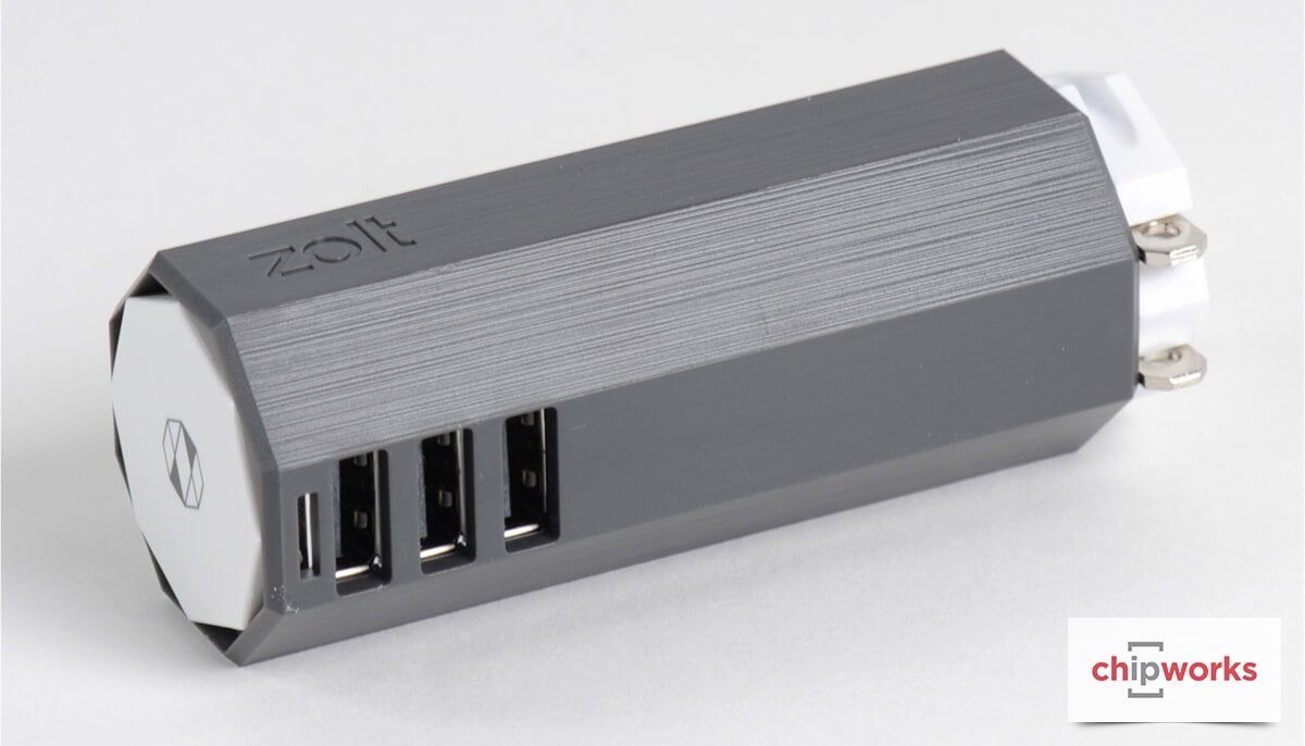
Avogy Zolt laptop charger SiC deviceWe do have one Zolt charger at PointThePower.com but we don’t have the lab to tear it down… Our friends from Chipworks did a very well job dismantling and revealing the inside of Zolt.  It was a striking news : Zolt contains an Avogy power device with a Cree1 Silicon Carbide MOSFET (repackaged by Avogy).

We were sure that GaN was the best device for this application, not SiC. And we are still sure about that. We thought that FINsix and Avogy managed to design their laptop charger using Super-Junction MOSFETs and fast smaller MOSFETs. It appears they did not. What option is left then? Silicon Carbide MOSFET.

But if you step back…

There are a few reasons that would lead one to go to SiC rather GaN, for now:

  1. Don’t trust GaN device makers: 600V is not available for production volumes!

Here are two examples to prove my word:

  • I recently read back interviews with two famous GaN makers stating 600V devices will be available by late 2014. We’re in 2016 now and the same makers do not have it yet.
  • I received an e-mail from a reader last year, pointing at a GaN power device announced in January. It disappeared from the catalog in May. We have no news since then.

I’m sure you all have similar examples in mind. So even if the GaN power device market says it’s ready, I want proofs that devices are available for this specific application. We will investigate these proofs in a market report to be released in April this year. We also have GaN devices teardown reports from our LTEC Corp., Our partner.

  1. Silicon Carbide MOSFET is expensive, but available and working

Chipworks Zolt Laptop charger SiC Cree mosfet

Chipworks’ picture of Zolt Laptop charger with SiC MOSFET

Avogy could order SiC MOSFETs and package them as flip-chip SMD. It seems devices switching faster than SJ-MOSFET was something required for their charger design. This is something possible with Silicon carbide if you are willing to pay the price. It’s a bit more difficult using GaN, even if you are in a wealthy company reading to lose some money.

  1. You don’t need the best charger, you need a working tinier charger… fast!

Have you seen FINSix Kickstarter campaign? I don’t blame them, I’m sure they did the work at its best and I know unexpected issues always rise in an engineering project. But similarly to other crowdfunding campaigns, they are late in the delivery of their Dart chargers. That makes backers a bit mad. Avogy managed to deliver less late compared to FINSix. They also designed something quite fast to make it available. This is a winning strategy that required to pick available devices: Silicon Carbide was the preferred solution.

Image capture of Finsix Dart laptop charger on kickstarter

Image capture of Finsix’s campaign on Kickstarter. See www.kickstarter.com

  1. LED and laptop charger market is about size: not efficiency, not lifetime, and not even price!

Yes: not even price. The chargers that we are talking about are expensive. A Zolt is 99 USD, Dart is about the same price. You have to add an extra 20 bucks if you own an Apple laptop. That is more expensive than Apple chargers, which are the most expensive laptop chargers on the market.

So, for a third-party charger this is very expensive. And with these 10 extra bucks you can definitely put a few dollars in a SiC device rather than struggling with a Super-Junction MOSFET. A third option would be to go for GaN, which will probably be cheaper than SiC when it’s available. We did miss that in our analysis of the situation.

There is also no need for a long lifetime as it’s targeting consumer electronics. These products have a maximum life of 3 to 5 years. Why would the charger last more?

Conclusion: SiC vs. GaN leaves SiC as a winner…in 2015

Again it’s all about availability. SiC has been around for 15 years. Gallium Nitride is much newer. So expecting GaN to be ready yet as SiC is still struggling to establish is quite optimistic. GaN will be ready and as of the characteristics we see, we expect it to eat a great amount of the market shares from Super Junction MOSFET. You get can get more information by downloading the sample of our market report: We will establish how, when and where is this market report to be published in April.
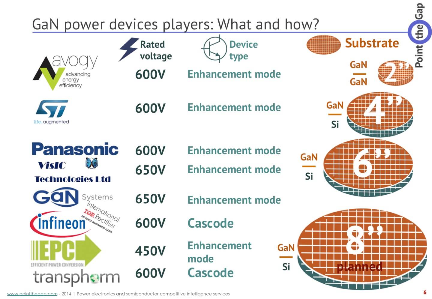
GaN-devices

Extract from PointThePower.com Market report to be released April 2016 – (c) Point The Gap

Combine all these reasons together and the best shot if you were designing a small charger using LLC resonant converter topology is either to go for Super Junction MOSFET and optimize cooling like hell… or put one SiC MOSFET die to ease your cooling and optimization design, and be sure you have devices to manufacture you chargers.

I have been working as a market analyst for a few years now, and I start to know about the market, about market players and their habits. There is a common habit in power devices market and start-up world: They are often optimistic.

PointThePower.com tries not to spread too much optimism: because it leads to disappointment.

Notes:

1: Cree has spin-off its RF and Power business units and merged it with APEI Inc, a company they acquired recently. The new entity is called Wolfspeed.


POWDEC has succeeded in making GaN PSJ (Polarized Super Junction) transistors on sapphire substrate having both 1,200 V rating-voltage and the on-resistance of less than 100 mΩ.

Powdec has developed a PSJ (Polarization Super-junction) structure instead of the FP (Field-Plate). The PSJ is so strong against the current collapse that sapphire can be used as substrate. As a result, the device is free from the electric breakdown caused by the substrate. And Powdec succeeded in obtaining up to 6 kV of the breakdown voltage for the device with GaN thickness as thin as 1 μm.

GaN-on-Si devices are applied to the conversion systems only below 600 V rating range. However, the present achievements using the unique PSJ-on-sapphire platform shows that the PSJ devices can enter into the application fields where Si-IGBTs dominate today.

What is Polarized Super Junction?

SJ (Super-junction) is a structure to improve both the conductivity and the breakdown voltage of the Si power-MOS transistor. The drift layer consists of thin p/n stacks while the conventional one consists of a single n-type layer. PSJ (Polarization Super-junction) is a method to implement the SJ effect in the GaN/AlGaN system where the polarization effect functions as SJ.

GaN-on-Silicon versus GaN-on-Sapphire:

Most GaN device makers develop GaN-on-Silicon (or GaN/Si) power devices. Powdec’s 1,200V devices are GaN-on-Sapphire devices. Not using the Silicon and using Sapphire implies intrinsic differences in the device structure and operation.

GaN-on-Si power devices:

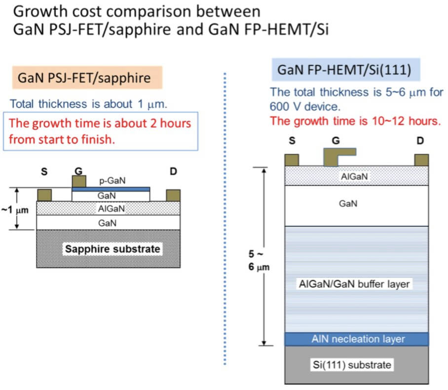
GaN power devices today are implemented on Si(111) substrate, which is called “GaN-on-Si” or “GaN/Si”. The thickness of the nitride layers needed for 600V rating devices is generally 5μm or more. The GaN/Si devices are equipped with Field-plates (FP are conductive plates set on the gate to split the steep electric field). FPs are indivisibly needed for the conductive Si substrate to mitigate the current collapses. Current-collapse is another name for the current decreasing phenomenon during the transistor operation. The channel electrons are scattered and deployed around the channel by the strong electric field. These immobile electrons act as the negative bias for the channel resulting in the decrease of the current.

Advantages of GaN-on-Sapphire for Power devices:

Powdec GaN on sapphire gallium nitride power devices PSJ super junctionSapphire substrate is also a common platform for GaN-LED production and the growth runs successively without chamber-cleaning. On the other hand, the growth on Si substrate needs chamber-cleaning prior to the deposition to avoid the unwanted chemical reactions between GaN and Si interface. The chamber-cleaning takes extra time and cost. As a whole, the throughput for GaN PSJ-FET/sapphire growth is roughly ten times larger than that of the GaN FP-HEMT/Si growth.

The thermal conductivity of sapphire, 40 [W/m K], is lower than that of Si, 150 [W/m K]. This problem is solved here by face-downing the die and contacting it on the base substrate, so that the heat can dissipate without going through the sapphire. As a result, the device has operated at as large as 8 amperes of the continuous current mode (CCM) under free standing (without fin) condition.


FINsix Corporation , the high-frequency power electronics design start-up, today announced its partnership with Lenovo, the PC manufacturer, to bring Lenovo’s laptops the smallest ever 65W charger option for ThinkPad laptops.

The two companies have collaborated under a joint development agreement, and Lenovo is set to offer the new charger, dubbed the ThinkPad 65W Adapter, as an option for the new ThinkPad X1 Carbon and X1 Yoga. FINsix and Lenovo will be exhibiting the new charger at CES, the global consumer electronics trade show, January 6-9 in Las Vegas.

FINsix is a company Point The Gap featured in its article about Gallium Nitride and consumer power adapters. It developped a laptop adapter using Resonant LLC converter topology to operate at higher frequency of conversion. This high frequency allows smaller passive components and better efficiency. It’s a technology transferred from RF and Military applications. FINsix was initially created on the campus of MIT, with the objective to power LED with their technology. They reoriented their aim to laptop adapters later, as a more accessible market. These technology will be featured in Point The Gap next market report about GaN devices and applications.

An interesting fact about this technology is that today’s FINsix adapters use Infineon Silicon based devices (CoolMOS and OptiMOS, respectively for high voltage and low voltage sides). But it could become and enabler and a first volume produced system to use Gallium Nitride power electronics devices. The topology fits perfectly the high frequency capabilities of GaN devices. It also compensates the youngness of GaN with the relatively short lifetime needed for a laptop charger.

“Lenovo is constantly searching for partners who have disruptive technologies that can add value to our customers,” said Luis Hernandez, vice president and general manager of Lenovo’s ThinkPad Business Unit. “We are working with FINsix because their power conversion technology is a game-changer. It brings a level of portability that we expect will become the standard of the future.”

Vanessa Green, CEO of FINsix, said,

“We are thrilled to partner with the market leader in personal computers. Lenovo has a strong customer base and this collaboration positions us to scale quickly among corporate customers eager to lighten their load when on the go.”

The ThinkPad 65W Micro Adapter is based on the same high-frequency power technology as FINsix’s first product, the Dart, a 65W aftermarket laptop adapter with a 2.1 amp USB port for simultaneously charging phones, tablets, and other devices. The Dart has been featured in a Kickstarter campaign about 18 months ago. Deliveries have been delayed many times and does not seem to have started yet. It was featured at CES in 2014.


The new facility produces and develops Insulated Gate Bipolar Transistor (IGBT) modules, which are terminal power semiconductor devices used as electronic switches that combine high efficiency and fast switching, IMI said in a statement.

They are used on trains, refrigerators, lamp ballasts, air-conditioners, solar applications, motion devices and anything that needs electric switching and requires power efficiency.


“The power module business is very much aligned with IMI’s strategy of offering innovative solutions which will impact our top and bottom lines. Further, it is in line with the expanding business in our target markets of automotive and industrial segments,” IMI President and Chief Executive Officer Arthur Tan was quoted in the statement as saying.

IMI is one of the few companies in the world capable of handling not only the electronics manufacturing side of the power modules but also the power semiconductor side of the business, Mr. Tan said.

Power modules are seen accounting for 30% of the total power of semiconductor market by 2019, IMI said.

Demand for modular power solutions from original equipment manufacturers is on the rise because of their higher power density and reliability, IMI said.

The company refurbished a surface mount technology assembly facility in Laguna Technopark into a power module facility, IMI Strategic Planning and Marketing Manager Frederick L. Blancas said.

IMI reported a 5% year-on-year jump in nine-month profit to $22 million despite a global economic slowdown and electronics industry downturn that pulled down consolidated revenues by 4% to $621.5 million.

Shares in IMI added four centavos or 0.69% to close at P5.80 each on Thursday.

Source

As part of the company’s strategy to move more significantly into power semiconductors for industrial and automotive markets, Littelfuse has made an investment in Monolith Semiconductor, Inc., a start-up company developing silicon carbide technology. Silicon carbide is a rapidly emerging semiconductor material that enables power devices to operate at higher switching frequencies and temperatures versus conventional silicon. This allows inverters and other energy conversion systems to be built with significantly improved power density, energy efficiency and cost.

“Investing in and partnering with Monolith’s experienced team of silicon carbide and power semiconductor experts allows us to quickly evolve our portfolio with strategically relevant and innovative technology,”

said Ian Highley, Littelfuse Senior VP and GM, Semiconductor Products, and CTO.

“Silicon carbide power technology is among the most promising advancements in the semiconductor market today. It will be an important tool in helping us solve complex problems for our customers.”

“Forming this strategic partnership with Littelfuse accelerates development and helps bring silicon carbide technology to the market,” said Sujit Banerjee, PhD, CEO of Monolith Semiconductor. “Littelfuse is an ideal partner for us. We are excited to dramatically increase our customer reach, gain access to global channels, and benefit from their sales and marketing depth and expertise.”

Initially this is not a material investment for Littelfuse; however, the company has committed to add to its investment once Monolith has achieved certain milestones. This investment is not expected to have any material financial impact on Littelfuse in 2015 or 2016.

About Littelfuse
Founded in 1927, Littelfuse is the world leader in protection with growing global platforms in power controls and sensing. The company serves global customers in the electronics, automotive and industrial markets with technologies including fuses, semiconductors, polymers, ceramics, relays and sensors. Littelfuse has over 8,000 employees in more than 35 locations throughout the Americas, Europe and Asia. For more information, please visit the Littelfuse website: Littelfuse.com.

About Monolith Semiconductor
Monolith Semiconductor Inc., a Round Rock, Texas-based startup company, is focused on improving the affordability and reliability of SiC power devices by utilizing advanced manufacturing techniques and high-performance processes and designs. For more information, please visit the Monolith Semiconductor website: monolithsemi.com.

Source

Raytheon UK’s foundry has received an order from a major fabless semiconductor manufacturer to mass produce silicon carbide (SiC) Schottky barrier diodes which are used for power conversion.

Raytheon UK’s Scottish facility will produce over 1,000 wafers in the first year. The customer will package the devices, which will have voltage ratings ranging from 600V to 1.7kV and current ratings ranging from 1 to 50A.

“This order demonstrates the increasing demand for silicon carbide semiconductors,” said John Kennedy, head of Raytheon UK’s Integrated Power Solutions.

“We have the process know-how and we’re adept at minimising the engineering costs. As an independent foundry, we have greater scope to find more innovative solutions for our customers.”

Raytheon UK’s Glenrothes foundry is the longest established independent full-scale production-qualified facility in Europe – if not the world – capable of SiC wafer processing. It has, for example, already fabricated Schottky and PiN diodes, as well as JFETs and MOSFETs, for other customers.

SiC properties include a breakdown electric field of 2,000kV/cm compared to silicon’s 300kV/cm – allowing for higher voltages; a bandgap energy of 3.26eV compared with silicon’s 1.12eV – enabling RUK007 Page 2 of 2 DECA-613 higher temperature operation; and excellent thermal conductivity (4.9W/cm.K compared with silicon’s
1.5W/cm.K).

source

World-leading nano-electronics research center imec announced today that it is extending its Gallium Nitride-on-Silicon (GaN-on-Si) R&D program, and is now offering joint research on GaN-on-Si 200mm epitaxy and enhancement mode device technology. The extended R&D initiative includes exploration of novel substrates to improve the quality of the epitaxial layers, new isolation modules to increase the level of integration, and the development of advanced vertical devices. Imec welcomes new partners interested in next generation GaN technologies and companies looking for low-volume manufacturing of GaN-on-Si devices to enable the next generation of more efficient and compact power converters.

“Since the program’s launch in July 2009, we have benefited from strong industry engagement, including participation from IDMs, epi-vendors and equipment and material suppliers. This underscores the industrial relevance of our offering,” stated Rudi Cartuyvels, executive vice president of smart systems at imec. “Interested companies are invited to become a partner and actively participate in our program. Imec’s open innovation model allows companies to have early access to next-generation devices and power electronics processes, equipment and technologies and speed up innovation at shared cost.”

GaN technology offers faster switching power devices with higher breakdown voltage and lower on-resistance than silicon, making it an outstanding material for advanced power electronic components. Imec’s R&D program on GaN-on-Si was launched to develop a GaN-on-Si process and bring GaN technology towards industrialization. Building on imec’s excellent track record in GaN epi-layer growth, new device concepts and CMOS device integration, imec has now developed a complete 200mm CMOS-compatible GaN process line. Imec’s GaN-on-Si technology is reaching maturity, and companies can gain access to the platform by joining imec’s GaN-on-Si industrial affiliation program (IIAP). The process line is also open to fabless companies interested in low-volume production of GaN-on-Si devices tailored to their specific needs, through dedicated development projects.

Imec’s portfolio includes three types of buffers optimized for breakdown voltage and low traps-related phenomena (i.e. current dispersion): a step graded AlGaN buffer, a super lattice buffer, and a buffer with low-temperature AlN interlayers. Imec explored side-by-side enhancement mode power devices of the MISHEMT and p-GaN HEMT type, as well as a gate-edge terminated Schottky power diode featuring low reverse leakage and low turn-on voltage.

The latest generation of imec enhancement mode power devices shows a threshold voltage beyond +2V, an on-resistance below 10 ohm mm and output current beyond 450 mA/mm. These devices represents the state of the art of enhancement mode power devices.

In this next phase of the GaN program, imec is focusing on further improving the performance and reliability of its current power devices, while in parallel pushing the boundaries of the technology through innovation in substrate technology, higher levels of integration and exploration of novel device architectures.

source

ON Semi’s offer of 20$ per share, representing a total of 2.4B$ as been beaten by a better offer.

The new bidder offered 21,70$ per share. The origin of the offer is still anonymous, and is being examined by Fairchild’s board. Several sources relate that the new offer comes from a group led by China Resources Holding.

Among the issues posed by selling Fairchild to a Chinese company, is the fact that the offer needs to be reviewed and approved by the CFIUS (Committee on Foreign Investment in the U.S.), an agency that has scuttled transactions involving Chinese SOEs. Phoenix based ON Semiconductor’s offer had the advantage to keep the US flag floating over Fairchild’s headquarter.

China’s willing to acquire Power semiconductor technology is not new. The country has been actively working on developing it’s own technologies. Even if they master now the manufacturing of IGBTs. They are still late as the technology used is quite old and not as advanced as the one you could find at power semiconductor dinosaurs like Infineon, Mitsubishi, and Fairchild. The development of T&D and Smartgrid needs as well as electric mobility put China in need of sourcing such technology.