Tag Archive for: Device

VisIC Technologies, a technology-leading developer of Gallium Nitride power semiconductors, previously announced the world’s lowest resistance 650V blocking voltage ALL-Switch product family specifying an Rdson as low as 15 mOhm.

VisIC Technologies has now delivered ALL-Switch Evaluation Boards (EB) and samples to leading customers. The EB allows customers to perform extensive testing confirming ALL-Switch’s leadership switching parameters.

The EB includes gate driver and switching control logic based upon commercially available components. ALL-Switch is configured for hard switching on the EB and can switch a 400V load with greater than 30A currents at over 500kHz. (See the attached oscilloscope trace.)

Meeting the highly demanding requirements of power switching with GaN has been the Holy Grail for power conversion research in the last decade. ALL-Switch is a product realization of that research.

VisIC’s technology solves problems that have limited devices from simultaneously achieving step function reductions in conduction and switching losses for power conversion systems that can benefit from high switching speeds.  VisIC’s products easily exceed the performance of competitive products using Silicon, Silicon Carbide or GaN.

VisIC will soon announce soon the details of a Half Bridge reference design.


Source


A new family of Power MOSFETs from STMicroelectronics allows designers of power supplies to maximize the power efficiency of their products while enhancing robustness and safety margins. The MDmeshTM K5 devices are the first in the world to combine the benefits of super-junction technology with a drain-to-source breakdown voltage of 1500V; they have already captured important design wins with major customers in Asia, Europe, and the USA.

The new devices address the growing demand for higher output power for auxiliary switched-mode power supplies in servers, where power-supply robustness is a key factor in minimizing down-time, and in industrial applications such as welding and factory automation. For these applications, where power output ranges from 75W to 230W or above, super-junction MOSFET technology is the preferred choice because of its outstanding dynamic-switching performance.

ST’s MDmesh K5 Power MOSFET family takes this technology to a new level, with the lowest On-Resistance (Rds(on)) per area and the lowest gate charge (Qg) in the market, resulting in the industry’s best FoM (Figure of Merit)1. The devices are ideal for all popular power-supply topologies, including standard, quasi-resonant and active-clamp flyback converters, and LLC2 half bridge converters for applications where high efficiency (up to 96%) and output powers approaching 200W are required for a wide range of input voltages.

The first two members of the new family are the STW12N150K5 and the STW21N150K5, which offer maximum drain-to-source currents of 7A and 14A, respectively, with gate charge as low as 47nC (STW12N150K5) or On-Resistance as low as 0.9Ω (STW21N150K5). Both devices are offered in TO-247 packages in volume quantities at prices of $14 for 1,000 units.

Integrated Device Technology, Inc. (IDT®) (IDTI) today announced an agreement to acquire privately held ZMDI (Zentrum Mikroelektronik Dresden AG) for total consideration of $310M in cash. The acquisition provides IDT with a highly regarded Automotive & Industrial business, and extends their technology leadership in high performance programmable power devices and timing & signal conditioning.

Automotive & Industrial provides a significant new growth opportunity. IDT gains immediate leverage for new designs in Wireless Charging, Power Management, and Timing & Signal Conditioning. ZMDI’s business is already well established and positioned for growth, and benefits immediately from IDT’s scale and technology.

“This move accelerates progress to our $800M annual revenue goal within our industry benchmark financial performance by over a year,” said Gregory Waters, IDT President & CEO. “IDT’s strategy is unchanged, but our product and technology position is significantly expanded. Our target market segments of Consumer, Communications, and High Performance Computing all benefit from additional product, revenue, and customer relationships that bolster our commitment to outgrow the semiconductor market by at least a factor of two.”

IDT extends their rapidly growing line of programmable power devices, with new high-power products addressing Communications Infrastructure and Data Center applications. This creates a new industry franchise for high performance, scalable power management solutions that cover applications ranging from Wireless Charging to Solid State Drives to Data Centers & 4G/5G basestations.

“We gain an exceptional group of talented people and intellectual property from ZMDI, who join one of the technology industry’s fastest growing companies. With the added benefit of IDT’s cost structure and high volume manufacturing capability, we expect ZMDIrevenues to achieve a similar financial model as IDT’s existing business in the first year of combined operations,” Waters added.

ZMDI’s signal conditioning products provide an elegant interface between microcontrollers and analog components, such as sensors. This is extremely complimentary to IDT’s Advanced Timing products, and will enable intelligent systems that are aware of their surroundings, and can adjust system performance, timing, and power management automatically.

“We’re enthusiastic to join with IDT, and create the best positioned product innovation team in the mixed-signal semiconductor industry,” said Thilo von Selchow, President and CEO of ZMDI. “It’s rare to see such a potent combination that not only provides a powerful financial result, but more importantly establish the product and technology teams that will lead the industry in innovative new products and growth for this decade.”

The transaction has been unanimously approved by the board of directors of both companies, with closing expected before calendar end.


Wolfspeed, the new spin-off from Cree, that makes silicon carbide (SiC) and gallium nitride (GaN) wide-bandgap semiconductor devices, has launched what it claims is the industry’s first 1700V SiC MOSFET offered in an optimized surface-mount (SMD) package. The higher blocking voltage enables design engineers to replace lower-rated silicon MOSFETs with the new SiC MOSFETs, delivering higher efficiency, simplified driver circuitry, and lower thermal dissipation, and resulting in lower total system costs, says the firm.

The new SMD package, specifically designed for high-voltage MOSFETs, has a small footprint with a wide creepage distance (7mm between drain and source). This is made possible by the small die size and high blocking capability of Wolfspeed’s SiC planar MOS technology. The new package also includes a separate driver source connection, which reduces gate ringing and provides clean gate signals.

“Our new 1700V SiC MOSFET provides power electronics engineers with significant design advantages, particularly in flyback topologies,”

claims Edgar Ayerbe, marketing manager for power MOSFETs. “Due to the lower switching losses of silicon carbide, the devices operate at much lower junction temperatures. This enables customers to directly mount the devices onto the PCB with no additional heat-sinks, which greatly reduces the manufacturing costs and improves the reliability of the systems,” he adds.

“The result is a smaller, lighter power supply with a lower system cost than is possible using silicon devices.”

Application of the new 1700V SiC MOSFET is anticipated in auxiliary power supplies within high-power inverters — such as solar power inverters, motor drives, uninterruptible power system (UPS) equipment, wind-energy converters, and traction power systems — which typically buck down DC voltages to operate system logic, protection circuitry, displays, network interface, and cooling fans. They can also be used in the power supplies of three-phase e-meters, or in any converter application that requires high blocking voltages and low capacitance.

Designated the C2M1000170J, the new 1700V SiC MOSFET features an avalanche rating greater than 1800V, and an RDS(on) on-resistance of 1Ω. These characteristics ensure reliable performance in flyback converter circuits, including those in noisy electrical environments such as those found in high-power inverters, says Wolfspeed. By enabling the design of single-switch flyback topologies from input voltages spanning 200V to 1000V, the 1700V SiC MOSFET simplifies the complex drive and snubber circuit elements required for silicon devices, the firm adds.

The C2M1000170J is fully qualified and available for sampling now.

Panasonic Corporation today announced that it developed gallium nitride (GaN) diodes that can not only operate at a high current that is four times greater than that tolerated by conventional silicon carbide (SiC) diodes*1, but also operate at low voltages by virtue of their low turn-on voltage. Production of the new diodes was made possible via a newly developed hybrid structure composed of separately embedded structure comprised of a low-voltage unit and a high-current-capable unit, in preparation for high voltage conditions.

Conventional silicon (Si) diodes are limited with regard to reducing switching losses. On the other hand, diodes based on SiC, a compound that is considered as a promising next-generation power semiconductor, as well as GaN, require an increased chip area to achieve high-current operations, thus posing limitations on the reduction of switching losses and size owing to increased operating frequencies.

GaN gallium nitride diode picture from panasonic

The newly produced GaN diodes have achieved simultaneous high-current operations and low threshold voltage, and thus can handle high currents even with a small chip area. The capacitance of the chip can therefore be reduced to achieve lower switching losses, allowing the device to operate at higher frequencies. As a result, use of GaN diodes in the voltage conversion circuits or inverter circuits of automotive or industrial equipment that requires high power can reduce system size due to high frequency operation.

This newly developed product has the following advantages.

・High-current operation: 7.6 kA/cm2 (approximately 4 times*1)
・Lower turn-on voltage: 0.8 V
・Low on-resistance (RonA): 1.3 mΩcm2 (approximately 50% reduction*1)

The diodes were created based on the following technologies.

Hybrid structure of GaN diodes with a trenched p-GaN layer:

We proposed a hybrid GaN diode with a p-type layer in which trenches are formed, and developed a processing technology that can remove a p-type layer on an n-type layer in a selective manner to achieve not only high-current operations and a low turn-on voltage but also a breakdown voltage of 1.6 kV.

Fabrication of Diodes on a low-resistance GaN substrate:

For this development, we used conductive GaN substrates with a low resistance, which have been commercially used in LEDs and semiconductor lasers and are expected to be adopted in power devices in the future, and established the technologies for the epitaxial growth and processing on a GaN substrate before forming diodes. A structure in which currents flow in the vertical direction enables a smaller chip area and lower resistance.

This work was partially supported by the Ministry of the Environment, Government of Japan.

The results of this development were presented at the 2015 International Conference on Solid State Devices and Materials , Sapporo, Japan (September, 2015).

(*1 Compared to an SiC diode with a rated voltage of 1,200 V)


Alpha and Omega Semiconductor Limited, a designer, developer and global supplier of a broad range of power semiconductors and power ICs, today announced that it has entered into a preliminary agreement with the state authority of Chongqing, China, to form a joint venture for a new state-of-the-art power semiconductor manufacturing facility in the Liangjiang New Area of Chongqing.

Under the proposed agreement, the initial capitalization of the joint venture is expected to be approximately $300 million. The Chongqing authority would own 49% of the venture’s equity and invest in cash. AOS would own 51% of the equity and contribute primarily its existing assembly and testing equipment as well as certain intellectual property related to the operation of the facility.

“We are excited that this joint venture with the authority of Chongqing offers the prospect of creating new competitive advantages that can fuel growth for both Chongqing and AOS,” said Dr. Mike Chang, chairman and CEO of AOS.

“We expect the venture to deliver significant cost savings for AOS and allow us to reduce our tangible assets as well as drive meaningful improvements in working capital and capital expenditures. We believe this partnership will open doors to new customers and expand our sales in China, and particularly in the Chongqing area. The venture represents an important step in our continuing strategy to improve long-term profitability by accelerating growth, reducing costs, and diversifying our offerings of power semiconductor products.”

The joint venture is expected to begin manufacturing operations in 2017. AOS will gradually move its assembly and testing equipment from the company’s existing facility in Shanghai to the lower-cost Chongqing region. We expect our AOS Shanghai will continue as a company’s supply chain management center and technology center for high-value products. At a later date, the joint venture expects to construct a 12-inch fabrication facility that is suited for the production of power semiconductors.

The parties are negotiating a definitive joint venture agreement setting forth in more detail the financial and business terms, as well as the timeline, of the proposed project, which is expected to be a multi-year commitment divided into several stages. The execution of the joint venture agreement will be subject to various conditions, including the relevant government agency review and approval.

Transphorm Inc, a GaN devices manufacturer, today announced a $70 million investment round led by  KKR. KKR’s investment follows initial rounds of funding from Kleiner Perkins Caufield and Byers, Foundation Capital, Google Ventures, Soros Quantum Strategic Partners, INCJ, Fujitsu, Transphorm will use this funding to support its growth, product innovation and expansion.

“Gallium Nitride is the most important new semiconductor in the world today”

To know more about Gallium-nitride manufacturers and Transphorm:

Check our presentation and map of GaN manufacturers

Gallium nitride devices players map

Today, Hua Hong Semiconductor, a pure-play 200mm foundry, announced that it has achieved mass production of its new-generation ultra-high voltage 0.5um 700V BCD series process platform with over 98% yield. This process platform mainly focuses on the applications of green energy such as AC-DC converters and LED lighting.

While maintaining the original cost advantage of at least 12 pieces per 1P1M (1 poly layer and 1 metal layer), the new process further integrates 7.5V CMOS, 20V/40V medium-voltage LDMOS and 200V to 700V high-voltage power LDMOS for a broader scope of ultra-high voltage options to meet the needs of different voltage applications. This solution can provide difference-oriented Junction Field-Effect Transistor (JFET) and high-voltage resistance devices for start-up circuits as well as a lot of other options.

“Hua Hong Semiconductor’s ultra-high voltage 700V BCD technology caters for the trend of energy saving. Supported by this process platform, the high-voltage, low-current LED lighting drivers have a very broad market prospect”

said Dr. Kong Weiran, Executive Vice President of Hua Hong Semiconductor,

“We intend to continue to further enhance our advanced and differentiated process technology portfolio applied to LED lighting to manufacture high-performance, cost-effective LED driver ICs. In the future, we will expand our advanced power management platform to offer a comprehensive suite of cost-effective solutions for customers.”

EPC corp. announce the extension of their power transistor portfolio with a high performance, wider pitch chip-scale package for ease of high volume manufacturing and enhanced compatibility with mature manufacturing processes and assembly lines.


The first in a new family of “Relaxed Pitch” devices,  the  EPC2029 80 V, 31 A eGaN  FET features a 1 mm bal l pitch.  The wider pitch allows for placement of additional and larger vias under the device to enable high current carrying capability despite the extremely small 4.6 mm x 2.6 mm footprint.

Compared to state-of-the art silicon power MOFSETs with similar on-resistance, the EPC2029 is smaller and has many times superior switching performance.  TheEPC2029 is ideal for applications such as high frequency DC-DC converters, synchronous rectification in DC/DC and AC/DC converters, motor drives, and class-D audio.

To simplify the evaluation process of this latest high performance eGaN FET, the EPC9046 development board, featuring two EPC2029 eGaN FETs in a half-bridge topology with onboard gate drive is available.  TheEPC9046 allows for easy “in circuit” performance evaluation of the EPC2029 by including all critical components and is laid out for optimal switching performance with additional area to add buck output filter components.

The new 80 V EPC2029 and corresponding development board EPC9046 are both available for immediate delivery from Digi-Key.

ON Semiconductor Corp., and Transphorm have announced a newly formed partnership to co-develop and co-market gallium nitride (GaN) based products and power system solutions for a variety of high voltage applications in the industrial, computing, telecom and networking sectors.

This strategic partnership leverages strengths inherent in both companies:

  • Transphorm is recognized as the first company to bring to market production qualified 600 volt (V) GaN on silicon transistors and has unrivalled experience working with this advanced technology.
  • ON Semiconductor is a leading supplier of energy efficient power solutions, provides significant expertise in system design, and offers an impressive portfolio that ranges from power discretes, high performance AC/DC controllers and integrated switchers to full custom ASIC power management solutions.

For power applications, GaN has been shown to deliver significant performance advantages compared to silicon based devices. The new generations of packaged products currently being co-developed by ON Semiconductor and Transphorm will provide reliable, qualified solutions that will enable designers to achieve previously unobtainable levels of efficiency and power density.

“ON Semiconductor clearly recognizes the inherent benefits that GaN technology can bring to the power electronics market and we are excited about partnering with a recognized and proven leader in this area in addition to pursuing our own GaN development work,”

said Bill Hall, executive vice president and general manager of ON Semiconductor’s Standard Products Group. “This important new collaboration strategically combines our impressive power system solution capabilities with Transphorm’s GaN expertise. Together we can bolster customer confidence in this new technology and accelerate broad market adoption.”

“Partnering with a leading power semiconductor company like ON Semiconductor reaffirms Transphorm’s GaN leadership and will provide our customers a broader set of GaN based products and solutions,” said Fumihide Esaka, CEO of Transphorm.

“This relationship is not only significant for faster penetration of GaN in the marketplace but also meaningful for the entire power conversion industry.”

The first co-developed solutions based on 600 V GaN transistors are expected to be available for sampling before the end of 2014. These solutions will address high power density applications in the 200 W to 1000 W power range for compact power supplies and adapters addressing the telecom and server markets. Under the terms of the partnership, the co-developed packaged transistor products will include low voltage MOSFET silicon from ON Semiconductor for the cascoded switch, and proven GaN high voltage High-Electron-Mobility Transistors (HEMT) from Transphorm. Co-packaging, assembly and test of the devices will be done at ON Semiconductor production facilities.

Power system reference designs will be provided to customers, enabling implementation of new solutions with GaN-based transistors and the high performance AC/DC controllers required to take full advantage of the technical benefits of GaN devices.

Source

Infineon Technologies and Panasonic Corporation have announced an agreement under which both companies will jointly develop Gallium nitride (GaN) devices based on Panasonic’s normally-off (enhancement mode) GaN on silicon transistor structure integrated into Infineon’s surface-mounted device (SMD) packages. In this context Panasonic has provided Infineon with a license of its normally-off GaN transistor structure.

This agreement will enable each company to manufacture GaN devices. Customers will have the added advantage of having two possible sources for compatible packaged GaN power switches

A setup not available for any other GaN on silicon device so far. Both parties have agreed not to disclose any further details of the contract. For the first time the companies will showcase samples of a 600V 70mΩ device in a DSO  (Dual Small Outline) package at the trade show Applied Power Electronics Conference and Exposition(APEC), which will be held in Charlotte, North Carolina, March 15-19, 2015.

GaN on silicon has been receiving significant attention as one of the next compound semiconductor technologies that will on the one hand enable high power density and therefore a smaller footprint (e.g., for power supplies and adapters), and on the other hand serve as a major key for energy efficiency improvement. In general, power devices based on GaN on silicon technology can be used in a wide range of fields, from high voltage industrial applications such as power supplies in server farms (a potential application of the showcased 600V GaN device) to low voltage applications such as DC-DC conversion (e.g., in high-end consumer goods).

GaN power device application in laptop chargers has been highlighted in our blog article: Is GaN’s power devices future in Laptop chargers.


Have you ever seen a Wide Band Gap semiconductor market report talking about laptop adaptors?

[Update 06/2016]: You want to know more about the GaN power devices market and applications? We have a market report released in June 2016, talking about that. Click here to see it!

Nobody I know and that has been working in the power electronics world, forecasted or even thought that WBG semiconductor success will come through a highly massive and common product and market as laptop chargers. They talked about power supplies and P-o-L. But they also pointed out the industrial or professional computing stuffs rather the charger in front of you right now.

Today, Laptop adaptors are massively using Super Junction MOSFET: These are MOSFETs at 600V or 900V using a specific design to enhance electron mobility (and thus efficiency and performance) beyond Silicon standards. They work, they are now massively and easily produced, they represent 61M$ market size just for laptops today and more than 900M$ over all applications. Infineon is moving product manufacturing to their brand new and bigger site in Dresden. SJ MOSFET just fit perfectly and do the job like hell. That is for today.
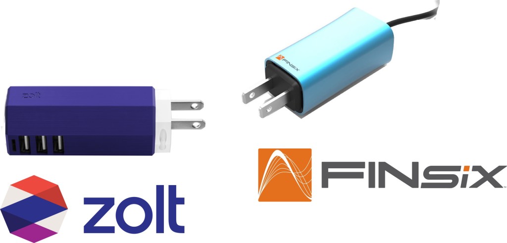
Zolt and finsix dart Gallium nitride based power supplies

Now let’s look at what power supplies start-ups are doing for tomorrow…

Similarly, I did not see many market reports on Wide band gap semiconductor talking about OnChip Power (former name of FINSix) and how they pivot from LED power supplies to laptop adaptors probably using Gallium Nitride power devices and high frequency conversion.

I have been following FINSix for a while, and have been curious, both professionally and personally, about their product: The Dart. It’s a real breakthrough they are working on. The same breakthrough that made transformers disappear to leave the place to Switch mode power supplies (SMPS) for portable devices. This was during the 90’s and allowed our chargers to become a little smaller, but mainly much lighter. You are not carrying hundreds of grams of a metal magnetic transformer anymore thanks to SMPS.

And FINSix is currently bringing high frequency conversion to the same public.

 We are now seeing another evolution, if not a revolution in the power adapter/charging world, that is very big for all Wide Band Gap community.

Watching Finsix make it’s way was enjoyable. I ended up learning that they were testing Transphorm GaN devices (for the most engineers among us: it’s a Cascode mounted Normally-On GaN-on-Silicon HeMT), together with an Infineon OptiMOS, to build a resonant converter. The real innovation was to transpose that topology, from military or aerospace, to mass production (Shipping has not begun yet…) for a public use.

They developed this tiny charger and managed to have enough publicity and buzz to build a company and a full business model around it. The first idea was to use the design for other purposes, but It seems that investors and deciding people thought money was somewhere else: between the wall plug and your laptop. Don’t misunderstand me: I think it’s a very good idea.

They completed a kickstarter campaign that worked very well ( almost 500,000$ and more than 4,000 pre-sales), attended several CES, and had their articles in CNet, TechCrunch, EnGadget, PCmag and a few other trendy-geeky website. They perfectly managed communication around the start-up and the product. The launch was a success; they got backed by VCs (5.2$M so far), and had media coverage.

Image capture of Finsix Dart laptop charger on kickstarter

Image capture of Finsix’s campaign on Kickstarter. See www.kickstarter.com

And you are going to ask me when is the GaN battle starting?

You don’t have a battle with a single player. And it did not take long before another GaN (Gallium Nitride) power devices manufacturer decided to build and sell their own product.

There was and there still is a battle in WBG, about which technology is best: Between GaN-on-GaN, GaN-on-Silicon or GaN-on-SiC. And the battle is still going on, with several start-up companies (GaN Systems, Transphorm, Avogy and a few others) developing and promoting their own technology.

But to win, you need to produce. You need to make your technology and your devices used in different systems. It’s the best proof that your stuff is working. And for your company to be successful, you need to sell.

Transphorm did well using that strategy. They communicated well. They managed to have their devices announced in PV inverters (with Yaskawa), motor drives, EV chargers and also these FinSix tiny laptop chargers.

And Avogy smelled the opportunity. What happened next? They also decided to develop, announce and produce their own tiny laptop charger.

Introduced during the last CES in January 2015, the Zolt was born. It’s a bit bulkier than Finsix Dart, but with extra USB ports. It’s announced to be shipped this summer and to be in the same price range the Dart is proposed: Zolt is 79USD pre-ordered or 99USD ortherwise, Dart is 89USD pre-ordered.

And that is what I call a battle. And I say, whoever the winner is, if he manage to sell to the mass, this will be a huge market breach for Wide Band Gap semiconductor to enter in our lives (at last…).

Gan products to be released illustration: Zolt, Finsix power supplies, yaskawa pv inverter, delta ev charger and toshiba LED power supply

Extract from PointThePower.com Market report on GaN for Power electronics.

So what if Wide Band Gap semiconductor future was laptop adaptors, and nobody saw it coming?

Now, we are at a situation where FinSiX has quite a lot of pre-order from Kickstarter to be honored while the release of the product is delayed again (to this summer) and people start to complain on Kickstarter’s comments board. The Dart is even part of The Verge’s “CES 2014 products that went nowhere”

On the other side, Avogy has created a very well designed website too, and is featured in The Verge with their Zolt charger, that is announced to be ready sooner than the Dart; even though they started later (And yet there is a big battle on the marketing and communication field).

I will have a lot of questions to ask during APEC Conference in March: Meeting with Avogy and Transphorm is already planned. (NDLR: We could not meet Avogy, but we met Vanessa Green, FinSix CEO in person, and the GaN devices based version does not seem to be current version. Maybe Dart 2.0 will be? and Transphorm’s devices are not the only one being under test).

And if one of these products is a success, it will provide a maximum visibility to GaN devices, and to the company doing it.

Avogy could easily put a “Avogy GaN inside” sticker, like Rohm did for the REFU-Sol PV inverter first featured SiC MOSFETS. This is the opportunity for them to gain visibility, market shares and cash. And we all know that a combination of these three is a very good first step to success.

So let’s watch and see: Which product is released first and is a commercial success? The answer to this two question is opening the door to GaN massive adoption in power electronics.


You thought you were a geek but you did not get a thing of what is said up here? Read this:


GaN, manufacturers and devices:
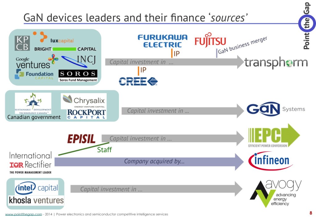
Gallium nitride power devices main manufacturers and their source for founding

Extract from PointThePower.com Market report on GaN for Power electronics.

GaN is a compound material made of Gallium and Nitride. It’s a semiconductor material called Wide Band Gap. Its gap being wide provides much better performances compared to silicon, traditionally used to design semiconductor devices, even in power electronics (for electric power conversion).

But producing GaN is a complicated and expensive process. Depending on how you do it and how cheap you want it, you end having a Silicon, a SiC (another Compound semiconductor) or GaN (polycrystal) to grow monocrystal GaN on top of it, Each having their pros and cons. This will be the subject of another article.