Tag Archive for: inverter

GaN again: good news?

I remember reading a tribune on TI social blog about how much GaN discussions were exhausting these days. The author said that APEC 2015 was hammering with GaN. We have been talking about GaN over and over. And every year it’s the same thing. 2015 Rap Session at APEC concluded once more that “It’s here, it’s coming. It’s good. We need to use it.” The round-table captivated the audience, as usual, but it leads to the same talks and questions with the same kind of people. I understand it becomes exhausting. It’s too much, even for me. I would like Gallium Nitride devices to be out, used everywhere, and that we start talking about something else, like Diamond or carbon nanotubes. I wish we had passed the curve, and we were at the top of it and we were looking at something else.

But we are not there yet. We will still see a lot of GaN, but I hope and I think that we will see different GaN. Let me explain why such a theory.

Why we will see GaN again at APEC this year

We already have device start-ups and bigger companies working on Gallium Nitride devices. We know the pros and cons. We know a lot about the devices themselves. So why would we still talk about that in 2016 at APEC? I wrote recently an article about why we still cannot find GaN in small power supplies (like Zolt and maybe FinSix). GaN devices will irrigate the market in the near future. You find all the analysis, explanations and some roadmap in the GaN Market Analysis report that we’re going to release next month. But there is still a missing thing: conversion systems (and the specialists that come with it).

And Point The Gap’s belief is that this is the next step for GaN. The step where you see big companies trying to use GaN devices, and where you see a few start-ups developing new types of systems. They work on new topologies, architectures, innovative passive components, PCB design or anything needed to make GaN or SiC deliver their best. This new era has started with FinSix  back when it was still On-Chip Power and they were targeting LED power supply business. Now you also have Cambridge Electronics Inc. in Massachusetts, or Nordic Power Converter in Denmark.

You also have companies like Navitas Semiconductor, which, even though they are still in stealth mode and will probably present more during APEC, claim on their single page website that they work on GaN power ICs.

Why is Gallium Nitride good news

We all want a “GaN break ”. But it’s very good news. It means a new era is coming. Now we have companies designing systems using GaN, and innovating at conversion level. Until now, all the power conversion topologies we have developed and invented were aimed at using Silicon. It started with Silicon MOSFET, then IGBT, and Super Junction MOSFET came after that to push further the limits of Silicon. Today, the performance of Silicon has been exploited, and even if we can still improve Si devices, the gain is not as large compared to what it was 10 or 20 years ago. GaN devices are available for sampling and soon for production, and now that system designers have something to work on, I think we will watch them play with it.

Thus we will hear about GaN because we are still expecting system design (and maybe passive components design) to show us what it got.

I bet we will see a few start-up companies going out of stealth mode, and these companies won’t talk about GaN devices. They will blow our mind with GaN based conversion systems. To me, it’s a heck of a good news!

All of this will of course be included in our “GaN devices and applications in power electronics” report, to be released by April of this year.

What else than GaN ?

SiC systems (and a few devices too)

We can definitely expect more Silico-Carbide devices. We have seen and we are seeing more and more systems using SiC MOSFETs. Not much using SiC BJT or other FET. We expect this trend to keep going on. Avogy proved that we can expect GaN and finally see SiC. Maybe it will happen again. PV inverters, UPS, Air conditioning built around full-SiC power modules and discrete devices is to expect this year at APEC.

In addition to that, this is the first year Wolfspeed will attend APEC as « Wolfspeed », grouping ex-Cree Power & RF together with ex-APEI Inc. This would be a good time to announce new projects, joint work or even high-end products. APEI Inc being very good at military or Hi-rel applications.

Power stacks for high-voltage applications are mostly announced during PCIM in May in Nuremberg. I thick we will wait a few more months for these announcements.

Passive components, power stacks or new inverters ?

We will probably have some new stuff on this side. But it’s not easy to define what will be announced in which field. There are some things going-on about digital control. Integration of passive components or Power IC is also fields where we expect to see tome new things announced.

Only time will tell. PointThePower.com will attend. We will be pleased to meet with you. Drop us an e-mail and we will come to you.

Otherwise, stay tuned on the website and you will live APEC as if you traveled, there through our report to come right after the show !

Google has finally released the name of Little Box Challenge winner. And the winner is… CE+T Power with it’s Red Electrical Devil’s team (named after the Belgium national soccer team). The judges from Google, IEEE Power Electronics and NREL declared them as far winners of the contest. Second place comes to Schneider Electric and third place to Virginia Tech’s Future Energy Electronics Center.

The Little Box Challenge was a contest launched by Google in July 2014. They promised a 1Million $ prize to whoever was capable of reaching a specific power density. As they described it, the objective was to shrink an Kilowatt-scale inverter in the size of a pizza box, which in other words, comes close to 50W/in³ or 3.05W/cm³.

We already talked about the challenge when it was announced and when the 18 finalists names were released. More than 2,000 teams registered for the competition and the committee reviewed and validated 80 proposals. The 18 finalists had to bring their inverters in person at NREL test lab and go under all listed validations and tests.

According to NREL, most competing teams used either Silicon Carbide (SiC) or Gallium Nitride (GaN) devices. This confirms that reaching this kind of specifications is made way easier using Wide Band Gap devices.

Schneider Electric, Virginia TEch and CE+T Power all built a 2kW inverter that passed all the tests (100 hours on a bench), and matched to the competition specifications. They not only managed to reach the 50W/in³ requirements and challenged it and went way over it.

Google little box challenge results ce+T power schneider electric


Faraday Future, the new Electric Vehicle start-up today announced to have developed and filed patents for high power density inverter. They claim to have increased power density by 20% to 30%.

The FF Echelon inverter patent is the first one to be approved and credited to Faraday Future: U.S. patent #9,241,428 B1

The Inverter was developed by the startup in-house engineering, and led by Senior Director of Electric Drive Silva Hiti.

“Condensing the number of transistors and other complex components enhances the inverter’s overall stability and dependability,” explained Silva Hiti, “allowing us to accomplish far more, with fewer materials.”

The official announcement states that FF team managed to minimize the number of components, both mechanical and electrical pieces, in order to achieve smaller size and higher reliability at the same time. They state that un-even sharing of current across electric components cause higher stress. An issue they solved by having less components to monitor and share current across.

Faraday Future FF Echelon power inverter

This design and method is opposite to the one used by Tesla when they designed and manufactured the first versions model S. As showed and explained in an article we published, Tesla preferred to use proven technology in its inverter, even if the number of IGBTs was high. Tesla used TO-247 discrete packaging for their power semiconductor devices, and managed to monitor and track current in each of these components.

Most Hybrid car manufacturer prefer to use power modules. Toyota designs and manufacture its own power modules and integrates them in the inverter, when most competitors will use Infineon, Mitsubishi Electric, or Danfoss power modules especially designed for electric and hybrid cars.


The new laboratory features a unique, large climate chamber capable of full power electrical testing in conditions simulating the arctic tundra to an equatorial rainforest. In addition, full verification and grid code requirements testing enable ABB to develop larger, more powerful inverters to meet the developing customer and industry trends.

A new multimillion dollar facility designed to test high power central photovoltaic (PV) inverters has been opened in Helsinki. The laboratory supports testing and verification of inverters for safe operation, endurance in a wide range of climatic conditions, compatibility to the most demanding renewables-specific grid code requirements, and to measure and test harmonics and grid interactions.Marc Gomez, Global Product Group Manager for solar inverters at ABB states:

“Our customers are asking for more powerful central inverters. They want to maximize their return on investment and connect more incoming PV power to one inverter. With this lab, we are able to test new inverter concepts, under varying weather conditions, and that allows us to deliver new innovation to our customers and ensure we lead the market.”

Climate testing can last several weeks for the equipment under test. Powered by a DC supply, the inverters are run at varying power levels with different simulated weather conditions to test inverter reliability. The climate chamber allows for accelerated product testing, important when the inverters are typically expected to operate for over 20 years. The climate chamber can vary temperatures from as low as -40°C to as high as +100°C, and relative humidity levels up to 95 percent.

ABB, a leading global supplier of solar photovoltaic inverters, provides the most comprehensive portfolio of products, systems, solutions and services along the solar PV value chain that enable the generation, transmission and distribution of solar power for grid-connected and microgrid applications. The portfolio includes inverters, low-voltage products, monitoring and control systems, grid connection, stabilization and integration products, as well as complete electrical balance of plant solutions. A wide range of support and maintenance services, including remote operations and diagnostics, help ensure solar installations deliver optimal performance.

Source

[Update 23/02/2016: We had several questions and feedback about this article. We would like to specify its context, hypothesis and boundaries. As specified in the title, this analysis is focusing on a specific application at a given time. We are talking about small laptop chargers for a design made during 2014 with a product released during 2015. This analysis is to change as fast as technologies, manufacturability and product availability will change. We would be happy to have your point of view as well. Please comment if you agree or disagree!]

Our last blog post about GaN in laptop chargers has been widely spread, read and appreciated (even in the French magazine electroniques.biz). On the other side it left some hypothesis, particularly on the type of devices used in these new FinSix Dart and Avogy Zolt laptop chargers. There was no information at the time. Device makers claimed they were suppliers but nothing could confirm it.

Zolt contains a SiC MOSFET from Cree:

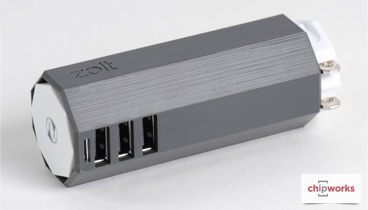
Avogy Zolt laptop charger SiC deviceWe do have one Zolt charger at PointThePower.com but we don’t have the lab to tear it down… Our friends from Chipworks did a very well job dismantling and revealing the inside of Zolt.  It was a striking news : Zolt contains an Avogy power device with a Cree1 Silicon Carbide MOSFET (repackaged by Avogy).

We were sure that GaN was the best device for this application, not SiC. And we are still sure about that. We thought that FINsix and Avogy managed to design their laptop charger using Super-Junction MOSFETs and fast smaller MOSFETs. It appears they did not. What option is left then? Silicon Carbide MOSFET.

But if you step back…

There are a few reasons that would lead one to go to SiC rather GaN, for now:

  1. Don’t trust GaN device makers: 600V is not available for production volumes!

Here are two examples to prove my word:

  • I recently read back interviews with two famous GaN makers stating 600V devices will be available by late 2014. We’re in 2016 now and the same makers do not have it yet.
  • I received an e-mail from a reader last year, pointing at a GaN power device announced in January. It disappeared from the catalog in May. We have no news since then.

I’m sure you all have similar examples in mind. So even if the GaN power device market says it’s ready, I want proofs that devices are available for this specific application. We will investigate these proofs in a market report to be released in April this year. We also have GaN devices teardown reports from our LTEC Corp., Our partner.

  1. Silicon Carbide MOSFET is expensive, but available and working

Chipworks Zolt Laptop charger SiC Cree mosfet

Chipworks’ picture of Zolt Laptop charger with SiC MOSFET

Avogy could order SiC MOSFETs and package them as flip-chip SMD. It seems devices switching faster than SJ-MOSFET was something required for their charger design. This is something possible with Silicon carbide if you are willing to pay the price. It’s a bit more difficult using GaN, even if you are in a wealthy company reading to lose some money.

  1. You don’t need the best charger, you need a working tinier charger… fast!

Have you seen FINSix Kickstarter campaign? I don’t blame them, I’m sure they did the work at its best and I know unexpected issues always rise in an engineering project. But similarly to other crowdfunding campaigns, they are late in the delivery of their Dart chargers. That makes backers a bit mad. Avogy managed to deliver less late compared to FINSix. They also designed something quite fast to make it available. This is a winning strategy that required to pick available devices: Silicon Carbide was the preferred solution.

Image capture of Finsix Dart laptop charger on kickstarter

Image capture of Finsix’s campaign on Kickstarter. See www.kickstarter.com

  1. LED and laptop charger market is about size: not efficiency, not lifetime, and not even price!

Yes: not even price. The chargers that we are talking about are expensive. A Zolt is 99 USD, Dart is about the same price. You have to add an extra 20 bucks if you own an Apple laptop. That is more expensive than Apple chargers, which are the most expensive laptop chargers on the market.

So, for a third-party charger this is very expensive. And with these 10 extra bucks you can definitely put a few dollars in a SiC device rather than struggling with a Super-Junction MOSFET. A third option would be to go for GaN, which will probably be cheaper than SiC when it’s available. We did miss that in our analysis of the situation.

There is also no need for a long lifetime as it’s targeting consumer electronics. These products have a maximum life of 3 to 5 years. Why would the charger last more?

Conclusion: SiC vs. GaN leaves SiC as a winner…in 2015

Again it’s all about availability. SiC has been around for 15 years. Gallium Nitride is much newer. So expecting GaN to be ready yet as SiC is still struggling to establish is quite optimistic. GaN will be ready and as of the characteristics we see, we expect it to eat a great amount of the market shares from Super Junction MOSFET. You get can get more information by downloading the sample of our market report: We will establish how, when and where is this market report to be published in April.

GaN-devices

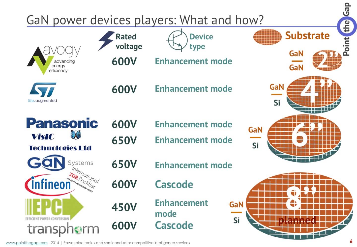
Extract from PointThePower.com Market report to be released April 2016 – (c) Point The Gap

Combine all these reasons together and the best shot if you were designing a small charger using LLC resonant converter topology is either to go for Super Junction MOSFET and optimize cooling like hell… or put one SiC MOSFET die to ease your cooling and optimization design, and be sure you have devices to manufacture you chargers.

I have been working as a market analyst for a few years now, and I start to know about the market, about market players and their habits. There is a common habit in power devices market and start-up world: They are often optimistic.

PointThePower.com tries not to spread too much optimism: because it leads to disappointment.

Notes:

1: Cree has spin-off its RF and Power business units and merged it with APEI Inc, a company they acquired recently. The new entity is called Wolfspeed.


Automotive electronics specialist HELLA, in collaboration with GaN Systems, and charging technology researchers at Kettering University’s Advanced Power Electronics Lab have developed a Level-2 electric vehicle (EV) charger prototype with efficiencies exceeding 97% at an unprecedented 2.6 kW/l power density. Prior to this achievement, Level-2 EV chargers reached maximum efficiencies of 94%. Using GaN Systems’ 60 A, 650 V GS66516T switches in an innovative two-stage architecture, the Kettering University research team, led by Associate Professor of Electrical Engineering, Dr. Kevin Bai, were able to increase the wall-to-battery efficiency to more than 3% greater than previously obtained.

HELLA’s Manager of Advanced Engineering, Matt McAmmond, added,

“The results of this collaboration are equally gratifying and commercially important, because they provide HELLA with a path to ultra-compact and lighter EV charger designs. In addition to benefiting HELLA and our customers, this development also has a positive environmental impact, as it represents another step toward the global effort to reduce power consumption.”

Dr. Bai and his team are known for collaborating with companies to help advance their charging technology. Commenting on the importance of this development, Dr. Bai said, “The switching performance we observed with the GaN Systems’ parts was marvelous. Using these devices our power electronics exhibited a power density greater than 2.6 kW/l. This is a significant milestone with important implications for charging electric vehicles, among other charging applications.” Dr. Bai characterized this development as a ‘game changer’ for the EV charging industry.


Gruppo PBM, a leader in industrial battery chargers, is using SiC MOSFETs in its new HF9 battery charger family to enable higher efficiency and power density at a lower overall system cost.

Demand for safe, efficient and fast-charging industrial batteries has increased exponentially along with the proliferation of power electronics. The HF9 product family is designed to provide the highest possible efficiency while achieving easy scalability for power ranging from six to 16 kilowatts. These benefits are made possible in part by Wolfspeed 1200V SiC MOSFET technology.

“We selected Wolfspeed SiC Planar MOSFETs for our new HF9 battery charger family because they enabled us to improve our battery chargers while achieving operational savings, increased productivity and increased safety. This was not possible with the best IGBTs in the market,”

said both Marco Mazzanti and Giancarlo Ceo, who respectively serve as CTO and R&D Engineer at Gruppo PBM.

Based in Italy, Gruppo PBM specializes in rugged high-frequency battery chargers, dischargers and testers. By using Wolfspeed SiC MOSFETs in its latest HF9 family, Gruppo PBM not only achieves improved efficiency, but also a reduction in component count, improving the overall reliability in the system by lowering the operating temperatures and—most importantly—reducing overall system cost.

“Wolfspeed’s SiC MOSFETs, especially our new C3M 900V family, are enjoying rapid adoption in the growing battery charger market segment,” explained Edgar Ayerbe, Wolfspeed’s power MOSFET marketing manager. “Our products increase power density and dramatically lower switching losses, making it possible to introduce smaller, cooler and lower cost chargers for the automotive and industrial markets.”

Sourcehttp://www.wolfspeed.com/news/gruppo-pbm

Game changing new technology delivers bi-directional AC/DC power flows, combining the functions of a rectifier, an inverter and a transfer technology in a single module.

Eltek is today announcing the launch of the Rectiverter, a power conversion module combining the functions of a rectifier, an inverter and a “static transfer switch” in one. The Rectiverter is a 3-port bidirectional converter that simplifies solutions providing both AC and DC power to critical loads in telecom, data center and industrial applications. It features a power conversion efficiency of 96% in mains mode and 94% when operating as an inverter.
Combining a rectifier, which converts AC to DC, and an inverter, which converts DC to AC into one box simplifies the power system complexity, reduces system size and improves overall system reliability, resulting in a reduced total cost of ownership over the product lifetime.

Eltek’s first product on the market is the Rectiverter HE, delivering 230V/1500W AC and 48V/1200W DC. It features high power conversion efficiency, and is controlled by a single Eltek Smartpack controller. Rectiverter systems are available as single or 3 phase, input and output, and can be scaled to meet any power demand.

“The Rectiverter is the first new technology development in modular power conversion for many years and it’s a big step into more efficient, more reliable power infrastructure,”

said Morten Schoyen, chief marketing officer of Eltek.

“It is a product that fits in well in applications where we today use rectifiers and inverters separately, and will open doors to new exciting opportunities”

“To integrate a rectifier and an Inverter in the same box, with bidirectional power flow and still maintain high efficiency is an impressive achievement,” said Dr. Tore M. Undeland, Prof Emeritus of Electrical Engineering at Norwegian University of Science and Technology (NTNU).
The Rectiverter first version is based on 48VDC and has a maximum capacity of 1500 VA for AC and 1200W of DC.  The total capacity of a module is 2000VA (AC and DC combined).

Source

The company HeSaLight has just booked no less than 50,000 power converters at Nordic Power Converters:

Nordic Power Converters is a spin-out company based on several years of technology development at DTU Electrical Engineering. The newly developed power converters that are both smaller and much more durable than traditional power converters are to be used in LED luminaires which HeSaLight manufactures.

The large order and a capital investment of DKK 13m from Seed Capital and 10 other investors means that Nordic Power Converters can now expand the business and hire more employees. Thus the company can really get started with producing tomorrow’s power converters, which could also replace the current big and bulky power converters for PCs for instance. Earlier this year Nordic Power Converters won Danish Tech Challenge – a competition for hardware-based companies and EU’s prize EIT Venture Award.

source

CRRC Yongji Xinshisu Electric Equipment Co., Ltd., a subsidiary of CRRC Corp. Ltd., has developed China’s own insulated gate bipolar transistor (IGBT) module of extra-high voltage level, which is of great significance for China to localize the high-speed rail and high-power locomotive technologies.

CRRC is the company born from merger of CNR (China Northern Railway) and CSR (China Southern Railway) which were among the biggest rolling stock manufacturers in the world.
The extra-high voltage 6500V/200A IGBT module has filled the blank of China in indigenous extra-high voltage IGBT module development and is to change the country’s dependency on IGBT imports, said Zou Shichang, academician of Chinese Academy of Sciences and chief technology officer of CRRC Corp.

China is the world’s largest IGBT consumer with an eight-billion-yuan market for IGBT consumption. However, the country hasn’t formed its own, complete, strong IGBT industrial system and the extra-high voltage IGBT chips have been monopolized by overseas enterprises.

Zou said the next move of CRRC is to promote the commercial application of 6500V/200A IGBT modules and further improvement in design, manufacturing, packaging, testing, and application of extra-high voltage IGBT chips, replace overseas IGBT modules with our own products, and to enhance the competitiveness of Chinese manufacturing industry in ‘going abroad’.

Today, 18 finalist teams for the Little Box Challenge, presented by Google and the IEEE Power Electronics Society, converged at the Energy Department’s National Renewable Energy Laboratory (NREL) to have their power inverters tested as part of a $1 million competition to build smaller devices for use in solar power systems.

“We’re very curious to see how the teams are tackling the different challenges that are inherent in trying to make inverter technology smaller and to see the performance of the final prototypes,” NREL Research Electrical Engineer Blake Lundstrom said. “The creativity and enthusiasm the teams bring to the competition is exciting and we hope some of the technical solutions will have long-term applications.”

More than 100 teams submitted technical approach documents and testing applications. On Oct. 21, each of the 18 finalists brought their inverters to the Energy Systems Integration Facility (ESIF) on the NREL campus in Golden, Colorado, to begin testing and evaluation. The day also included each team describing the highlights of its design and lessons learned to a team of researchers and engineers from Google, IEEE, NREL, and others in the power electronics industry.

NREL researchers have collaborated with Google and IEEE to assist in designing the specifications and evaluation methodology for the prototype inverters; each inverter’s efficiency and performance will be evaluated using the same set of typical operating conditions spanning 100 hours. Each inverter must be able to meet most of the same specifications required of inverters already available commercially.

The test results will help Google and IEEE decide the winner of the $1 million prize. To be successful, teams will have designed and built a residential-scale inverter with the highest power density – at least 50 watts per cubic inch. Currently, inverters are about the size of a picnic cooler and Google would like to see the technology shrink to the size of a small laptop computer, or smaller. Shrinking the inverter by 10 times or more and making it cheaper to produce and install would enable more solar-powered homes, more efficient distribution grids, and help bring electricity to remote areas.

The grand prize winner will be announced sometime in early 2016.

ESIF is the newest Energy Department user facility and the only one in the nation focused on integration of clean energy resources into the electric grid at utility scale. At ESIF, NREL offers industry partners access to award-winning, state-of-the art lab space, and a team of specialized scientists and engineers who provide advanced capabilities for research, development, and demonstration of key components of future energy systems.

The work was supported by funding from the Energy Department’s Office of Energy Efficiency and Renewable Energy in support of its SunShot Initiative. The SunShot Initiative is a collaborative national effort that aggressively drives innovation to make solar energy fully cost-competitive with traditional energy sources before the end of the decade. Through SunShot, the department supports efforts by private companies, universities, and national laboratories to drive down the cost of solar electricity to $0.06 per kilowatt-hour. Learn more at energy.gov/sunshot.

NREL is the U.S. Department of Energy’s primary national laboratory for renewable energy and energy efficiency research and development. NREL is operated for the Energy Department by The Alliance for Sustainable Energy, LLC.

Hitachi Ltd and Hitachi Automotive Systems Ltd developed a high-efficiency, high-output inverter for hybrid vehicles (HEVs) and electric vehicles (EVs).

Compared with Hitachi’s existing product, the power loss of the inverter is 60% smaller, and its electric power capacity per volume is about 100% larger. The two companies expect that the new inverter will realize a long drive range and improve acceleration performance.

This time, Hitachi and Hitachi Automotive Systems developed a full-SiC power module and an inverter equipped with the module for HEVs and EVs by using SiC/GaN parallel packaging technology and double-side-cooling power module technology that they developed in the past.

SiC silicon carbide for EV HEV from Hitachi

For example, the parallel packaging technology was used to equalize the timing of switching on/off each SiC power semiconductor. In other words, a circuit board that equalizes the length of the control signal line connected to each SiC power semiconductor was developed to equalize the resistance characteristics of circuits. As a result, it became possible to fully exploit the low-resistance properties of SiC power semiconductor, increasing power capacity.

Also, for the new inverter, circuits are stacked so that the directions of load currents become opposite to one another, and it is stored in the can-like metal cooling fin of the double-side-cooling power module. As a result, the cooling fin offsets the magnetic field generated by the circuits so that the magnetic field energy stored in the circuits is reduced.

The newly-developed double-side-cooling full-SiC power module will be exhibited at the 44th Tokyo Motor Show 2015, which will be open to the public from Oct 30, 2015, in Tokyo.


Source: http://techon.nikkeibp.co.jp/atclen/news_en/15mk/092900064/